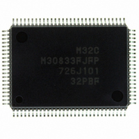
M30833FJFP#U5 Renesas Electronics America, M30833FJFP#U5 Datasheet - Page 291

M30833FJFP#U5
Manufacturer Part Number
M30833FJFP#U5
Description
IC M32C/83 MCU FLASH 100QFP
Manufacturer
Renesas Electronics America
Series
M16C™ M32C/80r
Datasheets
1.M3087BFLGPU3.pdf
(364 pages)
2.M30833FJGPU3.pdf
(96 pages)
3.M30833FJGPU3.pdf
(529 pages)
Specifications of M30833FJFP#U5
Core Processor
M32C/80
Core Size
16/32-Bit
Speed
32MHz
Connectivity
CAN, I²C, IEBus, SIO, UART/USART
Peripherals
DMA, WDT
Number Of I /o
85
Program Memory Size
512KB (512K x 8)
Program Memory Type
FLASH
Ram Size
31K x 8
Voltage - Supply (vcc/vdd)
3 V ~ 5.5 V
Data Converters
A/D 26x10b; D/A 2x8b
Oscillator Type
Internal
Operating Temperature
-20°C ~ 85°C
Package / Case
100-QFP
For Use With
R0K330879S001BE - KIT DEV RSK M32C/87R0K330879S000BE - KIT DEV RSK M32C/87
Lead Free Status / RoHS Status
Lead free / RoHS Compliant
Eeprom Size
-
Available stocks
Company
Part Number
Manufacturer
Quantity
Price
Part Number:
M30833FJFP#U5M30833FJFP#U3
Manufacturer:
Renesas Electronics America
Quantity:
135
Part Number:
M30833FJFP#U5M30833FJFP#U3
Manufacturer:
Renesas Electronics America
Quantity:
10 000
- Current page: 291 of 529
- Download datasheet (5Mb)
R
R
M
e
E
3
. v
J
2
Figure 21.17 Cascaded Connection
Figure 21.18 Counter Increment Mode (Group 0 and 1)
0
1
C
9
Two-phase pulse
3 .
B
8 /
signal is applied
INPC0j triggered by
the time measurement
0
1
3
Request by matching the base timer
0
3
J
G
4
a
0 -
o r
n
j=0 to 7, k=1,2,6,7
(1)
(2)
BT0S
3 .
1
BTS
u
f
Request from the INT pin
, 1
3
1
p
The IT in the GiBCR0 register (i=0,1) is set to "0" (bit 15 in the base timer overflows
The IT in the GiBCR0 register (i=0,1) is set to "1" (bit 14 in the base timer overflows
with the G0PO0 register
1
j=4,7,8,11 k=0 to 3
The above applies under the following conditions:
• The RST1 bit in the GiBCR1 register is set to "0" (the base timer is not reset by matching the base
• The UD1 to UD0 bits in the GiBCR1 register are set to "00
j=4,7,8,11 k=0 to 3
The above applies under the following conditions:
• The RST1 bit in the GiBCR1 register is set to "0" (the base timer is not reset by matching the base
• The UD1 to UD0 bits in the GiBCR1 register are set to "00
Request from group1
2
(
timer with the GiPO0 register)
timer with the GiPO0 register)
M
11
10
0
BCK1 to BCK0
BTkR bit in IIOjIR register
BTkR bit in IIOjIR register
0
3
6
2
C
Page 266
Base Timer i
8 /
b15 overflow signal
b14 overflow signal
Base Timer i
, 3
BT0S, BT1S : Bits in the BTSR register
BTS, CAS : Bits in the GiBCR1 register (i=0,1)
BCK1 to BCK0 : Bits in the GiBCR0 register (i = 0,1)
by 2(n+1)
M
Divider
3
2
C
f o
8 /
4000
8000
4
FFFF
C000
0000
FFFF
8000
0000
3
8
) T
8
16
16
"1"
"0"
"1"
"0"
16
16
16
16
"1"
16
"0"
"1"
"0"
G0TMj register
G0POj register
16
base timer
Group0
Request by matching the base timer
BT1S
INPC1k triggered by
the time measurement
BTS
Request from the INT pin
with the G1PO0 register
the group0 base timer
Request from group0
Bit 15 overflow in
f
BT1
2
2
" (counter increment mode)
" (counter increment mode)
0
1
0
1
CAS
CAS
G1TMj register
G1POj register
base timer
Group1
Write "0" by program
if setting to "0"
)
)
Write "0" by program
if setting to "0"
21. Intelligent I/O (Base Timer)
0
1
CAS
Waveform generation
match signal
Related parts for M30833FJFP#U5
Image
Part Number
Description
Manufacturer
Datasheet
Request
R

Part Number:
Description:
KIT STARTER FOR M16C/29
Manufacturer:
Renesas Electronics America
Datasheet:

Part Number:
Description:
KIT STARTER FOR R8C/2D
Manufacturer:
Renesas Electronics America
Datasheet:

Part Number:
Description:
R0K33062P STARTER KIT
Manufacturer:
Renesas Electronics America
Datasheet:

Part Number:
Description:
KIT STARTER FOR R8C/23 E8A
Manufacturer:
Renesas Electronics America
Datasheet:

Part Number:
Description:
KIT STARTER FOR R8C/25
Manufacturer:
Renesas Electronics America
Datasheet:

Part Number:
Description:
KIT STARTER H8S2456 SHARPE DSPLY
Manufacturer:
Renesas Electronics America
Datasheet:

Part Number:
Description:
KIT STARTER FOR R8C38C
Manufacturer:
Renesas Electronics America
Datasheet:

Part Number:
Description:
KIT STARTER FOR R8C35C
Manufacturer:
Renesas Electronics America
Datasheet:

Part Number:
Description:
KIT STARTER FOR R8CL3AC+LCD APPS
Manufacturer:
Renesas Electronics America
Datasheet:

Part Number:
Description:
KIT STARTER FOR RX610
Manufacturer:
Renesas Electronics America
Datasheet:

Part Number:
Description:
KIT STARTER FOR R32C/118
Manufacturer:
Renesas Electronics America
Datasheet:

Part Number:
Description:
KIT DEV RSK-R8C/26-29
Manufacturer:
Renesas Electronics America
Datasheet:

Part Number:
Description:
KIT STARTER FOR SH7124
Manufacturer:
Renesas Electronics America
Datasheet:

Part Number:
Description:
KIT STARTER FOR H8SX/1622
Manufacturer:
Renesas Electronics America
Datasheet:

Part Number:
Description:
KIT DEV FOR SH7203
Manufacturer:
Renesas Electronics America
Datasheet:


