M30833FJFP#U5 Renesas Electronics America, M30833FJFP#U5 Datasheet - Page 305
M30833FJFP#U5
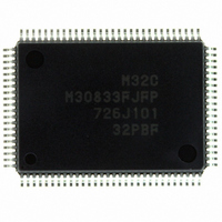
Manufacturer Part Number
M30833FJFP#U5
Description
IC M32C/83 MCU FLASH 100QFP
Manufacturer
Renesas Electronics America
Series
M16C™ M32C/80r
Datasheets
1.M3087BFLGPU3.pdf
(364 pages)
2.M30833FJGPU3.pdf
(96 pages)
3.M30833FJGPU3.pdf
(529 pages)
Specifications of M30833FJFP#U5
Core Processor
M32C/80
Core Size
16/32-Bit
Speed
32MHz
Connectivity
CAN, I²C, IEBus, SIO, UART/USART
Peripherals
DMA, WDT
Number Of I /o
85
Program Memory Size
512KB (512K x 8)
Program Memory Type
FLASH
Ram Size
31K x 8
Voltage - Supply (vcc/vdd)
3 V ~ 5.5 V
Data Converters
A/D 26x10b; D/A 2x8b
Oscillator Type
Internal
Operating Temperature
-20°C ~ 85°C
Package / Case
100-QFP
For Use With
R0K330879S001BE - KIT DEV RSK M32C/87R0K330879S000BE - KIT DEV RSK M32C/87
Lead Free Status / RoHS Status
Lead free / RoHS Compliant
Eeprom Size
-
Available stocks
Company
Part Number
Manufacturer
Quantity
Price

Part Number:
M30833FJFP#U5M30833FJFP#U3
Manufacturer:
Renesas Electronics America
Quantity:
135
Part Number:
M30833FJFP#U5M30833FJFP#U3
Manufacturer:
Renesas Electronics America
Quantity:
10 000


R
R
M
e
E
3
. v
J
2
0
Table 21.11 SR Waveform Output Mode Specifications (1/2)
NOTES:
Output Waveform
21.3.3 Set/Reset Waveform Output (SR Waveform Output) Mode (Group 0 to 3)
1
9
C
3 .
B
Output signal level of the OUTCij pin (i=0 to 3; j=0, 2, 4, 6) becomes "H" when the value of the base timer
matches that of the GiPOj register. The "H" signal switches to an "L" signal when the value of the base
timer matches that of the GiPOk register (k=j+1) or when the base timer is set to "0000
in the GiPOCRj register (j=0 to 7) is set to "1" (outputs "H" as initial value), an "H" signal is output when
waveform output starts. If the INV bit is set to "1" (output is inversed), the level of the waveform being
output is inversed. Table 21.11 lists specifications of SR waveform mode. Figure 21.26 shows an ex-
ample of a SR waveform mode operation.
1. When the GiPO0 register resets the base timer, the channel 0 and 1 SR waveform generation functions are not
2. When the INV bit in the GiPOCRj register is set to "1" (output inversed), the "L" width and "H" width are inversed.
3. Waveform from base timer reset until when output level becomes "H".
4. Waveform from when output level becomes "L" until base timer reset.
8 /
0
1
3
0
available.
3
J
G
4
a
0 -
n
o r
3 .
1
u
, 1
3
p
Item
1
2
(
M
0
0
3
(2)
6
2
C
Page 280
8 /
, 3
M
3
2
C
f o
8 /
4
3
8
• Free-running operation
• The base timer is reset by matching the base timer with the GiPO0 register
) T
8
(the RST2 to RST0 bits in the GiBCR1 register are set to "000
(1) m < n
(2) m
(the RST1 bit is set to "1", and the RST0 and RST2 bits are set to "0")
(1) m < n < p+2
(2) m < p+2
(3) If m
"H" width
"L" width
"H" width
"L" width
"H" width
"L" width
"H" width
"L" width
m : setting value of the GiPOj register (j=2, 4, 6)
n : setting value of the GiPOk register (k=j+1)
p : setting value of the GiPO0 register
m, n=0000
m : setting value of the GiPOj register (j=0, 2, 4, 6)
n : setting value of the GiPOk register (k=j+1)
m, n=0000
n
p+2, the output level is fixed to "L"
16
:
:
:
:
:
:
:
:
n
to FFFF
65536 - m
p + 2 - n
16
n - m
f
f
f
n-m
f
f
m
BTi
f
m
BTi
BTi
BTi
m
BTi
f
m
BTi
f
BTi
to FFFF
BTi
(3)
(3)
16
21. Intelligent I/O (Waveform Generation Function)
+
16
+
p=0001
Specification
p + 2 - n
65536 - n
f
16
BTi
f
BTi
to FFFD
(4)
(4)
16
2
16
")
". If the IVL bit
(1)
Related parts for M30833FJFP#U5
Image
Part Number
Description
Manufacturer
Datasheet
Request
R

Part Number:
Description:
KIT STARTER FOR M16C/29
Manufacturer:
Renesas Electronics America
Datasheet:

Part Number:
Description:
KIT STARTER FOR R8C/2D
Manufacturer:
Renesas Electronics America
Datasheet:

Part Number:
Description:
R0K33062P STARTER KIT
Manufacturer:
Renesas Electronics America
Datasheet:

Part Number:
Description:
KIT STARTER FOR R8C/23 E8A
Manufacturer:
Renesas Electronics America
Datasheet:

Part Number:
Description:
KIT STARTER FOR R8C/25
Manufacturer:
Renesas Electronics America
Datasheet:

Part Number:
Description:
KIT STARTER H8S2456 SHARPE DSPLY
Manufacturer:
Renesas Electronics America
Datasheet:

Part Number:
Description:
KIT STARTER FOR R8C38C
Manufacturer:
Renesas Electronics America
Datasheet:

Part Number:
Description:
KIT STARTER FOR R8C35C
Manufacturer:
Renesas Electronics America
Datasheet:

Part Number:
Description:
KIT STARTER FOR R8CL3AC+LCD APPS
Manufacturer:
Renesas Electronics America
Datasheet:
Part Number:
Description:
KIT STARTER FOR RX610
Manufacturer:
Renesas Electronics America
Datasheet:

Part Number:
Description:
KIT STARTER FOR R32C/118
Manufacturer:
Renesas Electronics America
Datasheet:

Part Number:
Description:
KIT DEV RSK-R8C/26-29
Manufacturer:
Renesas Electronics America
Datasheet:

Part Number:
Description:
KIT STARTER FOR SH7124
Manufacturer:
Renesas Electronics America
Datasheet:

Part Number:
Description:
KIT STARTER FOR H8SX/1622
Manufacturer:
Renesas Electronics America
Datasheet:

Part Number:
Description:
KIT DEV FOR SH7203
Manufacturer:
Renesas Electronics America
Datasheet: