M30833FJFP#U5 Renesas Electronics America, M30833FJFP#U5 Datasheet - Page 94
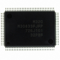
M30833FJFP#U5
Manufacturer Part Number
M30833FJFP#U5
Description
IC M32C/83 MCU FLASH 100QFP
Manufacturer
Renesas Electronics America
Series
M16C™ M32C/80r
Datasheets
1.M3087BFLGPU3.pdf
(364 pages)
2.M30833FJGPU3.pdf
(96 pages)
3.M30833FJGPU3.pdf
(529 pages)
Specifications of M30833FJFP#U5
Core Processor
M32C/80
Core Size
16/32-Bit
Speed
32MHz
Connectivity
CAN, I²C, IEBus, SIO, UART/USART
Peripherals
DMA, WDT
Number Of I /o
85
Program Memory Size
512KB (512K x 8)
Program Memory Type
FLASH
Ram Size
31K x 8
Voltage - Supply (vcc/vdd)
3 V ~ 5.5 V
Data Converters
A/D 26x10b; D/A 2x8b
Oscillator Type
Internal
Operating Temperature
-20°C ~ 85°C
Package / Case
100-QFP
For Use With
R0K330879S001BE - KIT DEV RSK M32C/87R0K330879S000BE - KIT DEV RSK M32C/87
Lead Free Status / RoHS Status
Lead free / RoHS Compliant
Eeprom Size
-
Available stocks
Company
Part Number
Manufacturer
Quantity
Price

Part Number:
M30833FJFP#U5M30833FJFP#U3
Manufacturer:
Renesas Electronics America
Quantity:
135
Part Number:
M30833FJFP#U5M30833FJFP#U3
Manufacturer:
Renesas Electronics America
Quantity:
10 000


R
R
M
e
E
3
. v
J
Figure 8.4 MCD Register
2
0
1
9
C
3 .
B
8 /
0
1
3
0
3
J
G
4
a
0 -
n
o r
Main Clock Division Register
b7
3 .
NOTES:
1
u
, 1
3
p
b6
1
1. Rewrite the MCD register after the PRC0 bit in the PRCR register is set to "1" (write enable).
2. While the microcomputer is in stop mode or low-power consumption mode, the MCD register is set to
3. Do not set to bit combinations not listed above.
4. Access CAN-associated register addresses (addresses 01E0
2
(
"08
register is set to "1"(X
register to "12
M
In on-chip oscillator mode, divide-by-8 mode cannot be entered even if the CM05 bit in the CM0
0
b5
0
3
6
16
2
b4
" (divide-by-8 mode).
C
8 /
b3
Page 69
, 3
b2
M
16
b1
3
" (no division mode).
2
C
b0
f o
8 /
IN
4
3
(b7 - b5)
8
MCD0
MCD1
MCD2
MCD3
MCD4
-X
Symbol
) T
8
Bit
OUT
Symbol
MCD
stopped).
Nothing is assigned. When write, set to "0".
When read, its content is indeterminate.
Main Clock Division
Select Bit
(1)
Bit Name
(2, 4)
Address
000C
16
b4 b3 b2 b1 b0
1 0 0 1 0 : Divide-by-1(no division)
0 0 0 1 0 : Divide-by-2 mode
0 0 0 1 1 : Divide-by-3 mode
0 0 1 0 0 : Divide-by-4 mode
0 0 1 1 0 : Divide-by-6 mode
0 1 0 0 0 : Divide-by-8 mode
0 1 0 1 0 : Divide-by-10 mode
0 1 1 0 0 : Divide-by-12 mode
0 1 1 1 0 : Divide-by-14 mode
0 0 0 0 0 : Divide-by-16 mode
16
to 0245
mode
16
After Reset
XXX01000
) after setting the MCD
Function
2
8. Clock Generation Circuit
(Note 3)
RW
RW
RW
RW
RW
RW
Related parts for M30833FJFP#U5
Image
Part Number
Description
Manufacturer
Datasheet
Request
R

Part Number:
Description:
KIT STARTER FOR M16C/29
Manufacturer:
Renesas Electronics America
Datasheet:

Part Number:
Description:
KIT STARTER FOR R8C/2D
Manufacturer:
Renesas Electronics America
Datasheet:

Part Number:
Description:
R0K33062P STARTER KIT
Manufacturer:
Renesas Electronics America
Datasheet:

Part Number:
Description:
KIT STARTER FOR R8C/23 E8A
Manufacturer:
Renesas Electronics America
Datasheet:

Part Number:
Description:
KIT STARTER FOR R8C/25
Manufacturer:
Renesas Electronics America
Datasheet:

Part Number:
Description:
KIT STARTER H8S2456 SHARPE DSPLY
Manufacturer:
Renesas Electronics America
Datasheet:

Part Number:
Description:
KIT STARTER FOR R8C38C
Manufacturer:
Renesas Electronics America
Datasheet:

Part Number:
Description:
KIT STARTER FOR R8C35C
Manufacturer:
Renesas Electronics America
Datasheet:

Part Number:
Description:
KIT STARTER FOR R8CL3AC+LCD APPS
Manufacturer:
Renesas Electronics America
Datasheet:
Part Number:
Description:
KIT STARTER FOR RX610
Manufacturer:
Renesas Electronics America
Datasheet:

Part Number:
Description:
KIT STARTER FOR R32C/118
Manufacturer:
Renesas Electronics America
Datasheet:

Part Number:
Description:
KIT DEV RSK-R8C/26-29
Manufacturer:
Renesas Electronics America
Datasheet:

Part Number:
Description:
KIT STARTER FOR SH7124
Manufacturer:
Renesas Electronics America
Datasheet:

Part Number:
Description:
KIT STARTER FOR H8SX/1622
Manufacturer:
Renesas Electronics America
Datasheet:

Part Number:
Description:
KIT DEV FOR SH7203
Manufacturer:
Renesas Electronics America
Datasheet: