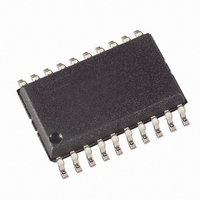
ATTINY26L-8SU Atmel, ATTINY26L-8SU Datasheet - Page 52

ATTINY26L-8SU
Manufacturer Part Number
ATTINY26L-8SU
Description
ID MCU AVR 2K 5V 8MHZ 20-SOIC
Manufacturer
Atmel
Series
AVR® ATtinyr
Specifications of ATTINY26L-8SU
Core Processor
AVR
Core Size
8-Bit
Speed
8MHz
Connectivity
USI
Peripherals
Brown-out Detect/Reset, POR, PWM, WDT
Number Of I /o
16
Program Memory Size
2KB (1K x 16)
Program Memory Type
FLASH
Eeprom Size
128 x 8
Ram Size
128 x 8
Voltage - Supply (vcc/vdd)
2.7 V ~ 5.5 V
Data Converters
A/D 11x10b
Oscillator Type
Internal
Operating Temperature
-40°C ~ 85°C
Package / Case
20-SOIC (7.5mm Width)
Package
20SOIC
Device Core
AVR
Family Name
ATtiny
Maximum Speed
8 MHz
Operating Supply Voltage
3.3|5 V
Data Bus Width
8 Bit
Number Of Programmable I/os
16
Interface Type
SPI/USI
On-chip Adc
11-chx10-bit
Number Of Timers
2
Cpu Family
ATtiny
Device Core Size
8b
Frequency (max)
8MHz
Total Internal Ram Size
128Byte
# I/os (max)
16
Number Of Timers - General Purpose
2
Operating Supply Voltage (typ)
3.3/5V
Operating Supply Voltage (max)
5.5V
Operating Supply Voltage (min)
2.7V
Instruction Set Architecture
RISC
Operating Temp Range
-40C to 85C
Operating Temperature Classification
Industrial
Mounting
Surface Mount
Pin Count
20
Package Type
SOIC
Processor Series
ATTINY2x
Core
AVR8
Data Ram Size
128 B
Maximum Clock Frequency
8 MHz
Maximum Operating Temperature
+ 85 C
Mounting Style
SMD/SMT
3rd Party Development Tools
EWAVR, EWAVR-BL
Development Tools By Supplier
ATAVRDRAGON, ATSTK500, ATSTK600, ATAVRISP2, ATAVRONEKIT
Minimum Operating Temperature
- 40 C
For Use With
ATSTK600-DIP40 - STK600 SOCKET/ADAPTER 40-PDIP770-1007 - ISP 4PORT ATMEL AVR MCU SPI/JTAG770-1004 - ISP 4PORT FOR ATMEL AVR MCU SPIATAVRISP2 - PROGRAMMER AVR IN SYSTEMATSTK505 - ADAPTER KIT FOR 14PIN AVR MCU
Lead Free Status / RoHS Status
Lead free / RoHS Compliant
Other names
ATTINY26L-8SJ
ATTINY26L-8SJ
ATTINY26L-8SJ
Available stocks
Company
Part Number
Manufacturer
Quantity
Price
Company:
Part Number:
ATTINY26L-8SU
Manufacturer:
Atmel
Quantity:
3 500
Part Number:
ATTINY26L-8SU
Manufacturer:
ATMEL/爱特梅尔
Quantity:
20 000
The masking alternate function is the pin usage as RESET. Digital input is enabled on pin PB7
also in SLEEP modes, if the pin change interrupt is enabled and not masked by the alternate
function.
• ADC9/INT0/T0/PCINT1 – Port B, Bit 6
ADC9: ADC Input Channel 9. Configure the port pins as inputs with the internal pull-ups
switched off to avoid the digital port function from interfering with the function of the analog to
digital converter.
INT0: External Interrupt source 0: The PB6 pin can serve as an external interrupt source
enabled by setting (one) the bit INT0 in the General Input Mask Register (GIMSK).
T0: Timer/Counter0 External Counter Clock input is enabled by setting (one) the bits CS02 and
CS01 in the Timer/Counter0 Control Register (TCCR0).
PCINT1: Pin Change Interrupt 1 pin. Pin change interrupt is enabled on pin when global interrupt
is enabled, pin change interrupt is enabled and the alternate functions do not mask the interrupt.
The masking alternate functions are the external low level Interrupt source 0 (INT0) and the
Timer/Counter0 External Counter clock input (T0). Digital input is enabled on pin PB6 also in
SLEEP modes, if the pin change interrupt is enabled and not masked by the alternate functions.
• ADC8/XTAL2/PCINT1 – Port B, Bit 5
ADC8: ADC Input Channel 8. Configure the port pins as inputs with the internal pull-ups
switched off to avoid the digital port function from interfering with the function of the analog to
digital converter.
XTAL2: Chip Clock Oscillator pin 2. Used as clock pin for all chip clock sources except internal
calibrateble RC Oscillator, external clock and PLL clock. When used as a clock pin, the pin can
not be used as an I/O pin. When using internal calibratable RC Oscillator, External clock or PLL
clock as Chip clock sources, PB5 serves as an ordinary I/O pin.
PCINT1: Pin Change Interrupt 1 pin. Pin change interrupt is enabled on pin when global interrupt
is enabled, pin change interrupt is enabled and the alternate functions do not mask the interrupt.
The masking alternate functions are the XTAL2 outputs. Digital input is enabled on pin PB5 also
in SLEEP modes, if the pin change interrupt is enabled and not masked by the alternate
functions.
• ADC7/XTAL1/PCINT1 – Port B, Bit 4
ADC7: ADC Input Channel 7. Configure the port pins as inputs with the internal pull-ups
switched off to avoid the digital port function from interfering with the function of the analog to
digital converter.
XTAL1: Chip Clock Oscillator pin 1. Used for all chip clock sources except internal calibrateble
RC oscillator and PLL clock. When used as a clock pin, the pin can not be used as an I/O pin.
When using internal calibratable RC Oscillator or PLL clock as chip clock sources, PB4 serves
as an ordinary I/O pin.
PCINT1: Pin Change Interrupt 1 pin. Pin change interrupt is enabled on pin when global interrupt
is enabled, pin change interrupt is enabled and the alternate functions do not mask the interrupt.
The masking alternate functions are the XTAL1 inputs. Digital input is enabled on pin PB4 also
in SLEEP modes, if the pin change interrupt is enabled and not masked by the alternate
functions.
• OC1B/PCINT0 – Port B, Bit 3
OC1B: Output Compare match output: The PB3 pin can serve as an output for the
Timer/Counter1 compare match B. The PB3 pin has to be configured as an output (DDB3 set
(one)) to serve this function. The OC1B pin is also the output pin for the PWM mode.
ATtiny26(L)
52
1477K–AVR–08/10


