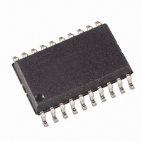
ATTINY26L-8SU Atmel, ATTINY26L-8SU Datasheet - Page 85

ATTINY26L-8SU
Manufacturer Part Number
ATTINY26L-8SU
Description
ID MCU AVR 2K 5V 8MHZ 20-SOIC
Manufacturer
Atmel
Series
AVR® ATtinyr
Specifications of ATTINY26L-8SU
Core Processor
AVR
Core Size
8-Bit
Speed
8MHz
Connectivity
USI
Peripherals
Brown-out Detect/Reset, POR, PWM, WDT
Number Of I /o
16
Program Memory Size
2KB (1K x 16)
Program Memory Type
FLASH
Eeprom Size
128 x 8
Ram Size
128 x 8
Voltage - Supply (vcc/vdd)
2.7 V ~ 5.5 V
Data Converters
A/D 11x10b
Oscillator Type
Internal
Operating Temperature
-40°C ~ 85°C
Package / Case
20-SOIC (7.5mm Width)
Package
20SOIC
Device Core
AVR
Family Name
ATtiny
Maximum Speed
8 MHz
Operating Supply Voltage
3.3|5 V
Data Bus Width
8 Bit
Number Of Programmable I/os
16
Interface Type
SPI/USI
On-chip Adc
11-chx10-bit
Number Of Timers
2
Cpu Family
ATtiny
Device Core Size
8b
Frequency (max)
8MHz
Total Internal Ram Size
128Byte
# I/os (max)
16
Number Of Timers - General Purpose
2
Operating Supply Voltage (typ)
3.3/5V
Operating Supply Voltage (max)
5.5V
Operating Supply Voltage (min)
2.7V
Instruction Set Architecture
RISC
Operating Temp Range
-40C to 85C
Operating Temperature Classification
Industrial
Mounting
Surface Mount
Pin Count
20
Package Type
SOIC
Processor Series
ATTINY2x
Core
AVR8
Data Ram Size
128 B
Maximum Clock Frequency
8 MHz
Maximum Operating Temperature
+ 85 C
Mounting Style
SMD/SMT
3rd Party Development Tools
EWAVR, EWAVR-BL
Development Tools By Supplier
ATAVRDRAGON, ATSTK500, ATSTK600, ATAVRISP2, ATAVRONEKIT
Minimum Operating Temperature
- 40 C
For Use With
ATSTK600-DIP40 - STK600 SOCKET/ADAPTER 40-PDIP770-1007 - ISP 4PORT ATMEL AVR MCU SPI/JTAG770-1004 - ISP 4PORT FOR ATMEL AVR MCU SPIATAVRISP2 - PROGRAMMER AVR IN SYSTEMATSTK505 - ADAPTER KIT FOR 14PIN AVR MCU
Lead Free Status / RoHS Status
Lead free / RoHS Compliant
Other names
ATTINY26L-8SJ
ATTINY26L-8SJ
ATTINY26L-8SJ
Available stocks
Company
Part Number
Manufacturer
Quantity
Price
Company:
Part Number:
ATTINY26L-8SU
Manufacturer:
Atmel
Quantity:
3 500
Part Number:
ATTINY26L-8SU
Manufacturer:
ATMEL/爱特梅尔
Quantity:
20 000
Functional
Descriptions
Three-wire Mode
1477K–AVR–08/10
The USI Three-wire mode is compliant to the Serial Peripheral Interface (SPI) mode 0 and 1, but
does not have the slave select (SS) pin functionality. However, this feature can be implemented
in software if necessary. Pin names used by this mode are: DI, DO, and SCK.
Figure 45. Three-wire Mode Operation, Simplified Diagram
Figure 45 shows two USI units operating in Three-wire mode, one as master and one as slave.
The two shift Registers are interconnected in such way that after eight SCK clocks, the data in
each register are interchanged. The same clock also increments the USI’s 4-bit counter. The
Counter Overflow (interrupt) flag, or USIOIF, can therefore be used to determine when a transfer
is completed. The clock is generated by the master device software by toggling the PB2 pin via
the PORTB Register or by writing a one to the USITC bit in USICR.
Figure 46. Three-wire Mode, Timing Diagram
The Three-wire mode timing is shown in Figure 46. At the top of the figure is a SCK cycle refer-
ence. One bit is shifted into the USI Shift Register (USIDR) for each of these cycles. The SCK
timing is shown for both external clock modes. In external clock mode 0 (USICS0 = 0), DI is
sampled at positive edges, and DO is changed (Data Register is shifted by one) at negative
edges. External clock mode 1 (USICS0 = 1) uses the opposite edges versus mode 0, i.e., sam-
CYCLE
SCK
SCK
SLAVE
MASTER
DO
DI
Bit7
Bit7
( Reference )
Bit6
Bit6
A
Bit5
Bit5
B
MSB
Bit4
Bit4
MSB
C
1
Bit3
Bit3
D
Bit2
Bit2
2
6
6
Bit1
Bit1
Bit0
Bit0
3
5
5
4
4
4
5
3
3
PORTBz
6
2
2
PBx
PBy
PBz
PBx
PBy
PBz
7
1
1
DO
DI
SCK
DO
DI
SCK
LSB
LSB
8
E
85


