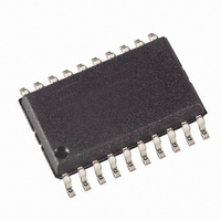
ATTINY26L-8SU Atmel, ATTINY26L-8SU Datasheet - Page 97

ATTINY26L-8SU
Manufacturer Part Number
ATTINY26L-8SU
Description
ID MCU AVR 2K 5V 8MHZ 20-SOIC
Manufacturer
Atmel
Series
AVR® ATtinyr
Specifications of ATTINY26L-8SU
Core Processor
AVR
Core Size
8-Bit
Speed
8MHz
Connectivity
USI
Peripherals
Brown-out Detect/Reset, POR, PWM, WDT
Number Of I /o
16
Program Memory Size
2KB (1K x 16)
Program Memory Type
FLASH
Eeprom Size
128 x 8
Ram Size
128 x 8
Voltage - Supply (vcc/vdd)
2.7 V ~ 5.5 V
Data Converters
A/D 11x10b
Oscillator Type
Internal
Operating Temperature
-40°C ~ 85°C
Package / Case
20-SOIC (7.5mm Width)
Package
20SOIC
Device Core
AVR
Family Name
ATtiny
Maximum Speed
8 MHz
Operating Supply Voltage
3.3|5 V
Data Bus Width
8 Bit
Number Of Programmable I/os
16
Interface Type
SPI/USI
On-chip Adc
11-chx10-bit
Number Of Timers
2
Cpu Family
ATtiny
Device Core Size
8b
Frequency (max)
8MHz
Total Internal Ram Size
128Byte
# I/os (max)
16
Number Of Timers - General Purpose
2
Operating Supply Voltage (typ)
3.3/5V
Operating Supply Voltage (max)
5.5V
Operating Supply Voltage (min)
2.7V
Instruction Set Architecture
RISC
Operating Temp Range
-40C to 85C
Operating Temperature Classification
Industrial
Mounting
Surface Mount
Pin Count
20
Package Type
SOIC
Processor Series
ATTINY2x
Core
AVR8
Data Ram Size
128 B
Maximum Clock Frequency
8 MHz
Maximum Operating Temperature
+ 85 C
Mounting Style
SMD/SMT
3rd Party Development Tools
EWAVR, EWAVR-BL
Development Tools By Supplier
ATAVRDRAGON, ATSTK500, ATSTK600, ATAVRISP2, ATAVRONEKIT
Minimum Operating Temperature
- 40 C
For Use With
ATSTK600-DIP40 - STK600 SOCKET/ADAPTER 40-PDIP770-1007 - ISP 4PORT ATMEL AVR MCU SPI/JTAG770-1004 - ISP 4PORT FOR ATMEL AVR MCU SPIATAVRISP2 - PROGRAMMER AVR IN SYSTEMATSTK505 - ADAPTER KIT FOR 14PIN AVR MCU
Lead Free Status / RoHS Status
Lead free / RoHS Compliant
Other names
ATTINY26L-8SJ
ATTINY26L-8SJ
ATTINY26L-8SJ
Available stocks
Company
Part Number
Manufacturer
Quantity
Price
Company:
Part Number:
ATTINY26L-8SU
Manufacturer:
Atmel
Quantity:
3 500
Part Number:
ATTINY26L-8SU
Manufacturer:
ATMEL/爱特梅尔
Quantity:
20 000
1477K–AVR–08/10
The ADC module contains a prescaler, which divides the system clock to an acceptable ADC
clock frequency.
The ADPS bits in ADCSR are used to generate a proper ADC clock input frequency from any
chip clock frequency above 100 kHz. The prescaler starts counting from the moment the ADC is
switched on by setting the ADEN bit in ADCSR. The prescaler keeps running for as long as the
ADEN bit is set, and is continuously reset when ADEN is low.
When initiating a conversion by setting the ADSC bit in ADCSR, the conversion starts at the fol-
lowing rising edge of the ADC clock cycle. If differential channels are selected, the conversion
will only start at every other rising edge of the ADC clock cycle after ADEN was set.
A normal conversion takes 13 ADC clock cycles. In certain situations, the ADC needs more
clock cycles to initialization and minimize offset errors. Extended conversions take 25 ADC clock
cycles and occur as the first conversion after the ADC is switched on (ADEN in ADCSR is set).
Special care should be taken when changing differential channels. Once a differential channel
has been selected, the gain stage may take as much as 125 µs to stabilize to the new value.
Thus conversions should not be started within the first 125 µs after selecting a new differential
channel. Alternatively, conversions results obtained within this period should be discarded. The
same settling time should be observed for the first differential conversion after changing ADC
reference (by changing the REFS1:0 bits in ADMUX).
The actual sample-and-hold takes place 1.5 ADC clock cycles after the start of a normal conver-
sion and 13.5 ADC clock cycles after the start of an extended conversion. When a conversion is
complete, the result is written to the ADC Data Registers, and ADIF is set. In Single Conversion
mode, ADSC is cleared simultaneously. The software may then set ADSC again, and a new
conversion will be initiated on the first rising ADC clock edge. In Free Running mode, a new con-
version will be started immediately after the conversion completes, while ADSC remains high.
Using Free Running mode and an ADC clock frequency of 200 kHz gives the lowest conversion
time, 65
Figure 53. ADC Timing Diagram, Extended Conversion (Single Conversion Mode)
Cycle Number
ADC Clock
ADEN
ADSC
ADIF
ADCH
ADCL
µs
, equivalent to 15 kSPS. For a summary of conversion times, see Table 43.
1
2
MUX and REFS
Update
12
13
14
15
Sample & Hold
16
Extended Conversion
17
18
19
20
21
22
Conversion
Complete
23
24
25
MSB of Result
LSB of Result
Next
Conversion
1
2
MUX and REFS
Update
3
97


