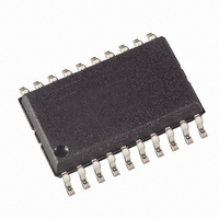
ATTINY26L-8SU Atmel, ATTINY26L-8SU Datasheet - Page 62

ATTINY26L-8SU
Manufacturer Part Number
ATTINY26L-8SU
Description
ID MCU AVR 2K 5V 8MHZ 20-SOIC
Manufacturer
Atmel
Series
AVR® ATtinyr
Specifications of ATTINY26L-8SU
Core Processor
AVR
Core Size
8-Bit
Speed
8MHz
Connectivity
USI
Peripherals
Brown-out Detect/Reset, POR, PWM, WDT
Number Of I /o
16
Program Memory Size
2KB (1K x 16)
Program Memory Type
FLASH
Eeprom Size
128 x 8
Ram Size
128 x 8
Voltage - Supply (vcc/vdd)
2.7 V ~ 5.5 V
Data Converters
A/D 11x10b
Oscillator Type
Internal
Operating Temperature
-40°C ~ 85°C
Package / Case
20-SOIC (7.5mm Width)
Package
20SOIC
Device Core
AVR
Family Name
ATtiny
Maximum Speed
8 MHz
Operating Supply Voltage
3.3|5 V
Data Bus Width
8 Bit
Number Of Programmable I/os
16
Interface Type
SPI/USI
On-chip Adc
11-chx10-bit
Number Of Timers
2
Cpu Family
ATtiny
Device Core Size
8b
Frequency (max)
8MHz
Total Internal Ram Size
128Byte
# I/os (max)
16
Number Of Timers - General Purpose
2
Operating Supply Voltage (typ)
3.3/5V
Operating Supply Voltage (max)
5.5V
Operating Supply Voltage (min)
2.7V
Instruction Set Architecture
RISC
Operating Temp Range
-40C to 85C
Operating Temperature Classification
Industrial
Mounting
Surface Mount
Pin Count
20
Package Type
SOIC
Processor Series
ATTINY2x
Core
AVR8
Data Ram Size
128 B
Maximum Clock Frequency
8 MHz
Maximum Operating Temperature
+ 85 C
Mounting Style
SMD/SMT
3rd Party Development Tools
EWAVR, EWAVR-BL
Development Tools By Supplier
ATAVRDRAGON, ATSTK500, ATSTK600, ATAVRISP2, ATAVRONEKIT
Minimum Operating Temperature
- 40 C
For Use With
ATSTK600-DIP40 - STK600 SOCKET/ADAPTER 40-PDIP770-1007 - ISP 4PORT ATMEL AVR MCU SPI/JTAG770-1004 - ISP 4PORT FOR ATMEL AVR MCU SPIATAVRISP2 - PROGRAMMER AVR IN SYSTEMATSTK505 - ADAPTER KIT FOR 14PIN AVR MCU
Lead Free Status / RoHS Status
Lead free / RoHS Compliant
Other names
ATTINY26L-8SJ
ATTINY26L-8SJ
ATTINY26L-8SJ
Available stocks
Company
Part Number
Manufacturer
Quantity
Price
Company:
Part Number:
ATTINY26L-8SU
Manufacturer:
Atmel
Quantity:
3 500
Part Number:
ATTINY26L-8SU
Manufacturer:
ATMEL/爱特梅尔
Quantity:
20 000
External
Interrupt
Pin Change
Interrupt
62
ATtiny26(L)
The External Interrupt is triggered by the INT0 pin. Observe that, if enabled, the interrupt will trig-
ger even if the INT0 pin is configured as an output. This feature provides a way of generating a
software interrupt. The External Interrupt can be triggered by a falling or rising edge, a pin
change, or a low level. This is set up as indicated in the specification for the MCU Control Regis-
ter – MCUCR. When the External Interrupt is enabled and is configured as level triggered, the
interrupt will trigger as long as the pin is held low.
The changed level is sampled twice by the Watchdog Oscillator clock, and if both these samples
have the required level, the MCU will wake up. The period of the Watchdog Oscillator is 1.0
(nominal) at 3.0V and 25°C. The frequency of the Watchdog Oscillator is voltage dependent as
shown in “Electrical Characteristics” on page 126.
The pin change interrupt is triggered by any change on any I/O pin of Port B and pins PA3, PA6,
and PA7, if the interrupt is enabled and alternate function of the pin does not mask out the inter-
rupt. The bit PCIE1 in GIMSK enables interrupt from pins PB[7:4], PA[7:6], and PA[3]. PCIE0
enables interrupt on digital pins PB[3:0].
The pin change interrupt is different from other interrupts in two ways. First, pin change interrupt
enable bits PCIE1 and PCIE0 also mask the flag if they are not set. The normal operation on
most interrupts is that the flag is always active and only the execution of the interrupt is masked
by the interrupt enable.
Secondly, please note that pin change interrupt is disabled for any pin that is configured as an
alternate function. For example, no pin change interrupt is generated from pins that are config-
ured as AREF, AIN0 or AIN1, OC1A, OC1A, OC1B, OC1B, XTAL1, or XTAL2 in a fuse selected
clock option, Timer0 clocking, or RESET function. See Table 30 for alternate functions which
mask the pin change interrupt and how the function is enabled. For example pin change inter-
rupt on the PB0 is disabled when USI Two-wire mode or USI Three-wire mode or
Timer/Counter1 inverted output compare is enabled.
If the interrupt is enabled, the interrupt will trigger even if the changing pin is configured as an
output. This feature provides a way of generating a software interrupt. Also observe that the pin
change interrupt will trigger even if the pin activity triggers another interrupt, for example the
external interrupt. This implies that one external event might cause several interrupts.
The value of the programmed fuse is “0” and unprogrammed is “1”. Each of the lines enables the
alternate function so “or” function of the lines enables the function.
1477K–AVR–08/10
µs


