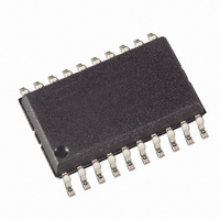
ATTINY26L-8SU Atmel, ATTINY26L-8SU Datasheet - Page 86

ATTINY26L-8SU
Manufacturer Part Number
ATTINY26L-8SU
Description
ID MCU AVR 2K 5V 8MHZ 20-SOIC
Manufacturer
Atmel
Series
AVR® ATtinyr
Specifications of ATTINY26L-8SU
Core Processor
AVR
Core Size
8-Bit
Speed
8MHz
Connectivity
USI
Peripherals
Brown-out Detect/Reset, POR, PWM, WDT
Number Of I /o
16
Program Memory Size
2KB (1K x 16)
Program Memory Type
FLASH
Eeprom Size
128 x 8
Ram Size
128 x 8
Voltage - Supply (vcc/vdd)
2.7 V ~ 5.5 V
Data Converters
A/D 11x10b
Oscillator Type
Internal
Operating Temperature
-40°C ~ 85°C
Package / Case
20-SOIC (7.5mm Width)
Package
20SOIC
Device Core
AVR
Family Name
ATtiny
Maximum Speed
8 MHz
Operating Supply Voltage
3.3|5 V
Data Bus Width
8 Bit
Number Of Programmable I/os
16
Interface Type
SPI/USI
On-chip Adc
11-chx10-bit
Number Of Timers
2
Cpu Family
ATtiny
Device Core Size
8b
Frequency (max)
8MHz
Total Internal Ram Size
128Byte
# I/os (max)
16
Number Of Timers - General Purpose
2
Operating Supply Voltage (typ)
3.3/5V
Operating Supply Voltage (max)
5.5V
Operating Supply Voltage (min)
2.7V
Instruction Set Architecture
RISC
Operating Temp Range
-40C to 85C
Operating Temperature Classification
Industrial
Mounting
Surface Mount
Pin Count
20
Package Type
SOIC
Processor Series
ATTINY2x
Core
AVR8
Data Ram Size
128 B
Maximum Clock Frequency
8 MHz
Maximum Operating Temperature
+ 85 C
Mounting Style
SMD/SMT
3rd Party Development Tools
EWAVR, EWAVR-BL
Development Tools By Supplier
ATAVRDRAGON, ATSTK500, ATSTK600, ATAVRISP2, ATAVRONEKIT
Minimum Operating Temperature
- 40 C
For Use With
ATSTK600-DIP40 - STK600 SOCKET/ADAPTER 40-PDIP770-1007 - ISP 4PORT ATMEL AVR MCU SPI/JTAG770-1004 - ISP 4PORT FOR ATMEL AVR MCU SPIATAVRISP2 - PROGRAMMER AVR IN SYSTEMATSTK505 - ADAPTER KIT FOR 14PIN AVR MCU
Lead Free Status / RoHS Status
Lead free / RoHS Compliant
Other names
ATTINY26L-8SJ
ATTINY26L-8SJ
ATTINY26L-8SJ
Available stocks
Company
Part Number
Manufacturer
Quantity
Price
Company:
Part Number:
ATTINY26L-8SU
Manufacturer:
Atmel
Quantity:
3 500
Part Number:
ATTINY26L-8SU
Manufacturer:
ATMEL/爱特梅尔
Quantity:
20 000
SPI Master Operation
Example
86
ATtiny26(L)
ples data at negative and changes the output at positive edges. The USI clock modes
corresponds to the SPI data mode 0 and 1.
Referring to the timing diagram (Figure 46.), a bus transfer involves the following steps:
1. The slave device and master device sets up its data output and, depending on the proto-
2. The master generates a clock pulse by software toggling the SCK line twice (C and D).
3. Step 2. is repeated eight times for a comlpete register (byte) transfer.
4. After eight clock pulses (i.e., 16 clock edges) the counter will overflow and indicate that
The following code demonstrates how to use the USI module as a SPI master:
The code is size optimized using only 8 instructions (+ ret). The code example assumes that the
DO and SCK pins are enabled as output in the DDRB Register. The value stored in register r16
prior to the function is called is transferred to the slave device, and when the transfer is com-
pleted the data received from the slave is stored back into the r16 register.
The second and third instructions clears the USI Counter Overflow Flag and the USI counter
value. The fourth and fifth instruction set Three-wire mode, positive edge Shift Register clock,
count at USITC strobe, and toggle SCK (PORTB2). The loop is repeated 16 times.
col used, enables its output driver (mark A and B). The output is set up by writing the
data to be transmitted to the serial Data Register. Enabling of the output is done by set-
ting the corresponding bit in the port data direction register (DDRB2). Note that point A
and B does not have any specific order, but both must be at least one half SCK cycle
before point C where the data is sampled. This must be done to ensure that the data
setup requirement is satisfied. The 4-bit counter is reset to zero.
The bit value on the slave and master’s data input (DI) pin is sampled by the USI on the
first edge (C), and the data output is changed on the opposite edge (D). The 4-bit counter
will count both edges.
the transfer is completed. The data bytes transferred must now be processed before a
new transfer can be initiated. The overflow interrupt will wake up the processor if it is set
to Idle mode. Depending of the protocol used the slave device can now set its output to
high impedance.
SPITransfer:
SPITransfer_loop:
out
ldi
out
ldi
out
sbis
rjmp
in
ret
USIDR,r16
r16,(1<<USIOIF)
USISR,r16
r16,(1<<USIWM0)+(1<<USICS1)+(1<<USICLK)+(1<<USITC)
USICR,r16
USISR,USIOIF
SPITransfer_loop
r16,USIDR
1477K–AVR–08/10


