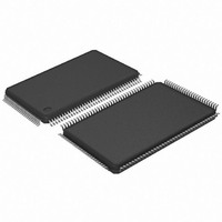
AT91SAM7SE32-AU Atmel, AT91SAM7SE32-AU Datasheet - Page 145

AT91SAM7SE32-AU
Manufacturer Part Number
AT91SAM7SE32-AU
Description
MCU ARM 32K HS FLASH 128-LQFP
Manufacturer
Atmel
Series
AT91SAMr
Specifications of AT91SAM7SE32-AU
Core Processor
ARM7
Core Size
16/32-Bit
Speed
55MHz
Connectivity
EBI/EMI, I²C, SPI, SSC, UART/USART, USB
Peripherals
Brown-out Detect/Reset, POR, PWM, WDT
Number Of I /o
88
Program Memory Size
32KB (32K x 8)
Program Memory Type
FLASH
Ram Size
8K x 8
Voltage - Supply (vcc/vdd)
1.65 V ~ 1.95 V
Data Converters
A/D 8x10b
Oscillator Type
Internal
Operating Temperature
-40°C ~ 85°C
Package / Case
128-LQFP
Controller Family/series
AT91SAM7xxxx
No. Of I/o's
88
Ram Memory Size
8KB
Cpu Speed
48MHz
No. Of Timers
3
Rohs Compliant
Yes
Processor Series
AT91SAMx
Core
ARM7TDMI
Data Bus Width
32 bit
Data Ram Size
8 KB
Interface Type
EBI, SPI, TWI, USART
Maximum Clock Frequency
55 MHz
Number Of Programmable I/os
88
Number Of Timers
3
Maximum Operating Temperature
+ 85 C
Mounting Style
SMD/SMT
3rd Party Development Tools
JTRACE-ARM-2M, KSK-AT91SAM7S-PL, MDK-ARM, RL-ARM, ULINK2
Development Tools By Supplier
AT91SAM-ICE, AT91-ISP, AT91SAM7SE-EK
Minimum Operating Temperature
- 40 C
On-chip Adc
10 bit, 8 Channel
For Use With
AT91SAM7SE-EK - EVAL BOARD FOR AT91SAM7SEAT91SAM-ICE - EMULATOR FOR AT91 ARM7/ARM9
Lead Free Status / RoHS Status
Lead free / RoHS Compliant
Eeprom Size
-
Lead Free Status / Rohs Status
Details
Available stocks
Company
Part Number
Manufacturer
Quantity
Price
Company:
Part Number:
AT91SAM7SE32-AU
Manufacturer:
ATMEL
Quantity:
624
Part Number:
AT91SAM7SE32-AU
Manufacturer:
ATMEL/爱特梅尔
Quantity:
20 000
- Current page: 145 of 655
- Download datasheet (8Mb)
Table 21-4.
21.6.5.3
6222B–ATARM–26-Mar-07
Mode
Attribute Memory
Common Memory
I/O Mode
Task File
Data Register
Control Register
Alternate Status Read
Drive Address
Standby Mode or
Address Space is not
assigned to CF
Read/Write Signals
CFCE1 and CFCE2 Truth Table
In I/O mode and True IDE mode, the CompactFlash logic drives the read and write command
signals of the SMC on CFIOR and CFIOW signals, while the CFOE and CFWE signals are deac-
tivated. Likewise, in common memory mode and attribute memory mode, the SMC signals are
driven on the CFOE and CFWE signals, while the CFIOR and CFIOW are deactivated.
21-4 on page 146
presents the signal decoding.
Attribute memory mode, common memory mode and I/O mode are supported by setting the
address setup and hold time on the NCS4 (and/or NCS2) chip select to the appropriate values.
For details on these signal waveforms, please refer to the section: Setup and Hold Cycles of the
Static Memory Controller Section.
CFCE2
NUB
NUB
NUB
1
1
1
1
0
0
1
CFCE1
shows a schematic representation of this logic and
NLB
NLB
NLB
0
0
0
0
1
1
1
Alternate True IDE Mode
AT91SAM7SE512/256/32 Preliminary
True IDE Mode
16 bits
16 bits
16 bits
16bits
DBW
8 bits
8 bits
8 bits
Don’t
8 bits
Don’t
Care
Care
Comment
Access to Even Byte on D[7:0]
Access to Even Byte on D[7:0]
Access to Odd Byte on D[15:8]
Access to Odd Byte on D[7:0]
Access to Even Byte on D[7:0]
Access to Odd Byte on D[15:8]
Access to Odd Byte on D[7:0]
Access to Even Byte on D[7:0]
Access to Odd Byte on D[7:0]
Access to Even Byte on D[7:0]
Access to Odd Byte on D[15:8]
Access to Even Byte on D[7:0]
Access to Odd Byte on D[7:0]
Don’t Care
Table 21-5 on page 146
Don’t Care
SMC Access Mode
Byte Select
Byte Select
Don’t Care
Byte Select
Don’t Care
Don’t Care
Byte Select
Don’t Care
Don’t Care
Figure
145
Related parts for AT91SAM7SE32-AU
Image
Part Number
Description
Manufacturer
Datasheet
Request
R

Part Number:
Description:
KIT EVAL FOR ARM AT91SAM7S
Manufacturer:
Atmel
Datasheet:

Part Number:
Description:
MCU, MPU & DSP Development Tools KICKSTART KIT ATMEL AT91SAM7S
Manufacturer:
IAR Systems

Part Number:
Description:
DEV KIT FOR AVR/AVR32
Manufacturer:
Atmel
Datasheet:

Part Number:
Description:
INTERVAL AND WIPE/WASH WIPER CONTROL IC WITH DELAY
Manufacturer:
ATMEL Corporation
Datasheet:

Part Number:
Description:
Low-Voltage Voice-Switched IC for Hands-Free Operation
Manufacturer:
ATMEL Corporation
Datasheet:

Part Number:
Description:
MONOLITHIC INTEGRATED FEATUREPHONE CIRCUIT
Manufacturer:
ATMEL Corporation
Datasheet:

Part Number:
Description:
AM-FM Receiver IC U4255BM-M
Manufacturer:
ATMEL Corporation
Datasheet:

Part Number:
Description:
Monolithic Integrated Feature Phone Circuit
Manufacturer:
ATMEL Corporation
Datasheet:

Part Number:
Description:
Multistandard Video-IF and Quasi Parallel Sound Processing
Manufacturer:
ATMEL Corporation
Datasheet:

Part Number:
Description:
High-performance EE PLD
Manufacturer:
ATMEL Corporation
Datasheet:

Part Number:
Description:
8-bit Flash Microcontroller
Manufacturer:
ATMEL Corporation
Datasheet:

Part Number:
Description:
2-Wire Serial EEPROM
Manufacturer:
ATMEL Corporation
Datasheet:


