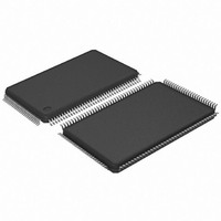
AT91SAM7SE32-AU Atmel, AT91SAM7SE32-AU Datasheet - Page 621

AT91SAM7SE32-AU
Manufacturer Part Number
AT91SAM7SE32-AU
Description
MCU ARM 32K HS FLASH 128-LQFP
Manufacturer
Atmel
Series
AT91SAMr
Specifications of AT91SAM7SE32-AU
Core Processor
ARM7
Core Size
16/32-Bit
Speed
55MHz
Connectivity
EBI/EMI, I²C, SPI, SSC, UART/USART, USB
Peripherals
Brown-out Detect/Reset, POR, PWM, WDT
Number Of I /o
88
Program Memory Size
32KB (32K x 8)
Program Memory Type
FLASH
Ram Size
8K x 8
Voltage - Supply (vcc/vdd)
1.65 V ~ 1.95 V
Data Converters
A/D 8x10b
Oscillator Type
Internal
Operating Temperature
-40°C ~ 85°C
Package / Case
128-LQFP
Controller Family/series
AT91SAM7xxxx
No. Of I/o's
88
Ram Memory Size
8KB
Cpu Speed
48MHz
No. Of Timers
3
Rohs Compliant
Yes
Processor Series
AT91SAMx
Core
ARM7TDMI
Data Bus Width
32 bit
Data Ram Size
8 KB
Interface Type
EBI, SPI, TWI, USART
Maximum Clock Frequency
55 MHz
Number Of Programmable I/os
88
Number Of Timers
3
Maximum Operating Temperature
+ 85 C
Mounting Style
SMD/SMT
3rd Party Development Tools
JTRACE-ARM-2M, KSK-AT91SAM7S-PL, MDK-ARM, RL-ARM, ULINK2
Development Tools By Supplier
AT91SAM-ICE, AT91-ISP, AT91SAM7SE-EK
Minimum Operating Temperature
- 40 C
On-chip Adc
10 bit, 8 Channel
For Use With
AT91SAM7SE-EK - EVAL BOARD FOR AT91SAM7SEAT91SAM-ICE - EMULATOR FOR AT91 ARM7/ARM9
Lead Free Status / RoHS Status
Lead free / RoHS Compliant
Eeprom Size
-
Lead Free Status / Rohs Status
Details
Available stocks
Company
Part Number
Manufacturer
Quantity
Price
Company:
Part Number:
AT91SAM7SE32-AU
Manufacturer:
ATMEL
Quantity:
624
Part Number:
AT91SAM7SE32-AU
Manufacturer:
ATMEL/爱特梅尔
Quantity:
20 000
- Current page: 621 of 655
- Download datasheet (8Mb)
AT91SAM7SE32 SPI Timings
Notes:
6222B–ATARM–26-Mar-07
Symbol
SPI
SPI
SPI
SPI
SPI
SPI
SPI
SPI
SPI
SPI
SPI
SPI
0
1
2
3
4
5
6
7
8
9
10
11
1. 3.3V domain: V
2. 1.8V domain: V
3. t
CPMCK
Parameter
MISO Setup time before SPCK rises (master)
MISO Hold time after SPCK rises (master)
SPCK rising to MOSI Delay (master)
MISO Setup time before SPCK falls (master)
MISO Hold time after SPCK falls (master)
SPCK falling to MOSI Delay (master)
SPCK falling to MISO Delay (slave)
MOSI Setup time before SPCK rises (slave)
MOSI Hold time after SPCK rises (slave)
SPCK rising to MISO Delay (slave)
MOSI Setup time before SPCK falls (slave)
MOSI Hold time after SPCK falls (slave)
: Master Clock period in ns.
VDDIO
VDDIO
Note that in SPI master mode the ATSAM7SE512/256/32 does not sample the data (MISO) on
the opposite edge where data clocks out (MOSI) but the same edge is used as shown in
40-4
from 3.0V to 3.6V, maximum external capacitor = 40 pF.
from 1.65V to 1.95V, maximum external capacitor = 20 pF.
and
Figure
40-5.
AT91SAM7SE512/256/32 Preliminary
3.3V domain
1.8V domain
3.3V domain
1.8V domain
3.3V domain
1.8V domain
3.3V domain
1.8V domain
3.3V domain
1.8V domain
3.3V domain
1.8V domain
3.3V domain
1.8V domain
3.3V domain
1.8V domain
3.3V domain
1.8V domain
3.3V domain
1.8V domain
3.3V domain
1.8V domain
3.3V domain
1.8V domain
Conditions
(1)
(2)
(1)
(2)
(1)
(2)
(1)
(2)
(1)
(2)
(1)
(2)
(1)
(2)
(1)
(2)
(1)
(2)
(1)
(2)
(1)
(2)
(1)
(2)
26 + (t
45 + (t
26 + (t
34 + (t
Min
CPMCK
CPMCK
CPMCK
CPMCK
0
0
0
0
1
1
3
3
1
1
3
3
)/2
)/2
)/2
)/2
(3)
(3)
(3)
(3)
Max
23.7
12
42
24
40
4
4
6
Units
ns
ns
ns
ns
ns
ns
ns
ns
ns
ns
ns
ns
ns
ns
ns
ns
ns
ns
ns
ns
ns
ns
ns
Figure
621
Related parts for AT91SAM7SE32-AU
Image
Part Number
Description
Manufacturer
Datasheet
Request
R

Part Number:
Description:
KIT EVAL FOR ARM AT91SAM7S
Manufacturer:
Atmel
Datasheet:

Part Number:
Description:
MCU, MPU & DSP Development Tools KICKSTART KIT ATMEL AT91SAM7S
Manufacturer:
IAR Systems

Part Number:
Description:
DEV KIT FOR AVR/AVR32
Manufacturer:
Atmel
Datasheet:

Part Number:
Description:
INTERVAL AND WIPE/WASH WIPER CONTROL IC WITH DELAY
Manufacturer:
ATMEL Corporation
Datasheet:

Part Number:
Description:
Low-Voltage Voice-Switched IC for Hands-Free Operation
Manufacturer:
ATMEL Corporation
Datasheet:

Part Number:
Description:
MONOLITHIC INTEGRATED FEATUREPHONE CIRCUIT
Manufacturer:
ATMEL Corporation
Datasheet:

Part Number:
Description:
AM-FM Receiver IC U4255BM-M
Manufacturer:
ATMEL Corporation
Datasheet:

Part Number:
Description:
Monolithic Integrated Feature Phone Circuit
Manufacturer:
ATMEL Corporation
Datasheet:

Part Number:
Description:
Multistandard Video-IF and Quasi Parallel Sound Processing
Manufacturer:
ATMEL Corporation
Datasheet:

Part Number:
Description:
High-performance EE PLD
Manufacturer:
ATMEL Corporation
Datasheet:

Part Number:
Description:
8-bit Flash Microcontroller
Manufacturer:
ATMEL Corporation
Datasheet:

Part Number:
Description:
2-Wire Serial EEPROM
Manufacturer:
ATMEL Corporation
Datasheet:


