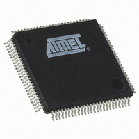
AT91SAM7X512-AU Atmel, AT91SAM7X512-AU Datasheet - Page 671

AT91SAM7X512-AU
Manufacturer Part Number
AT91SAM7X512-AU
Description
MCU ARM 512K HS FLASH 100-LQFP
Manufacturer
Atmel
Series
AT91SAMr
Datasheet
1.AT91SAM7X512-AU-999.pdf
(687 pages)
Specifications of AT91SAM7X512-AU
Core Processor
ARM7
Core Size
16/32-Bit
Speed
55MHz
Connectivity
CAN, Ethernet, I²C, SPI, SSC, UART/USART, USB
Peripherals
Brown-out Detect/Reset, DMA, POR, PWM, WDT
Number Of I /o
62
Program Memory Size
512KB (512K x 8)
Program Memory Type
FLASH
Ram Size
128K x 8
Voltage - Supply (vcc/vdd)
1.65 V ~ 1.95 V
Data Converters
A/D 8x10b
Oscillator Type
Internal
Operating Temperature
-40°C ~ 85°C
Package / Case
100-LQFP
Processor Series
AT91SAMx
Core
ARM7TDMI
Data Bus Width
32 bit
Data Ram Size
128 KB
Interface Type
CAN, SPI, SSC, TWI, USART, USB
Maximum Clock Frequency
55 MHz
Number Of Programmable I/os
13
Number Of Timers
3
Operating Supply Voltage
3 V to 3.6 V
Maximum Operating Temperature
+ 85 C
Mounting Style
SMD/SMT
3rd Party Development Tools
JTRACE-ARM-2M, KSK-AT91SAM7X-PL, MDK-ARM, RL-ARM, ULINK2
Development Tools By Supplier
AT91SAM-ICE, AT91-ISP, AT91SAM7X-EK
Minimum Operating Temperature
- 40 C
On-chip Adc
10 bit
No. Of I/o's
62
Ram Memory Size
128KB
Cpu Speed
55MHz
No. Of Timers
3
No. Of Pwm Channels
4
Digital Ic Case Style
LQFP
Rohs Compliant
Yes
For Use With
AT91SAM-ICE - EMULATOR FOR AT91 ARM7/ARM9AT91SAM7X-EK - KIT EVAL FOR AT91SAM7X256/128
Lead Free Status / RoHS Status
Lead free / RoHS Compliant
Eeprom Size
-
Lead Free Status / Rohs Status
Lead free / RoHS Compliant
Available stocks
Company
Part Number
Manufacturer
Quantity
Price
Company:
Part Number:
AT91SAM7X512-AU
Manufacturer:
Atmel
Quantity:
10 000
Company:
Part Number:
AT91SAM7X512-AU
Manufacturer:
ATMEL
Quantity:
717
- Current page: 671 of 687
- Download datasheet (11Mb)
6120H–ATARM–17-Feb-09
Version
6120G
Comments
Overview,
“Features”, TWI updated to include Atmel TWI compatibility with I
Section 7.4 ”Peripheral DMA Controller”
Section 10.8 ”Two-wire
Section 10.11 ”Timer Counter”
Section 10.15 ”Analog-to-Digital Converter”
CAN,
versa have been inverted.
Debug and Test,
Section 12.5.5 ”ID Code
DBGU,
Section 26.5.10 ”Debug Unit Chip ID
“SRAMSIZ: Internal SRAM Size” on page 226
Corrected bin values for 0x60 and 0xF0 and Architecture Identifier bit description for CAP7, AT91SAM7AQxx
Series and CAP11 in the bit description,
EMAC,
Section 37.5.3 “Network Status Register” on page
Section 37.3 “Functional Description” on page
FFPI,
Table
Global update to terms listed below:
Fuse → GPNVM
SFB → SGPB
CFB → CGPB
GFB → GGPB
Section 20.2.5.6 on page 126
PIO,
Section 27.4.5 “Synchronous Data Output” on page
Section 27.6 “Parallel Input/Output Controller (PIO) User Interface” on page
PIO_PSR, PIO_ODSR, PIO_PDSR in Register Mapping table.
PMC,
Section 25.3 ”Processor Clock Controller”
Figure 24-2,”Typical Crystal Connection”
PWM,
Section 33.6 “Pulse Width Modulation Controller (PWM) User Interface” on page
33-2, Register Mapping ; the PWM channel-dependent registers listed as indexed registers.
See
Section 33.6.11 ”PWM Channel Period
Section 33.6.13 ”PWM Channel Update
SPI,
Section 28.6.4 “SPI Slave Mode” on page
SPI_RDR.
Section 33.6.9 ”PWM Channel Mode
Figure 36-7,”Line Error Mode”
20-6,
Table
20-9,
Interface”, updated.
Table 20-18
Register”, product part numbers and JTAG ID code values updated.
&
The TC has Two output compare or one input capture per channel.
Section 20.3.4.6 on page
Conditions to switch from Error Active mode to Error Passive mode and vice
updated
Register”, SRAM bit description added for AT91SAM7L in the bit field.
Register”,
Register”;
updated with PDC priorities.
“ARCH: Architecture Identifier” on page 227
updated, removed C
Register”,
....the processor clock can be disabled by writing.... PMC_SDR.
265, corrected information on OVRES (SPI_SR) and data read in
AT91SAM7X512/256/128 Preliminary
INL and DNL updated.
564, Added information on clocks in first paragraph.
Section 33.6.12 ”PWM Channel Counter
584, Corrected status for IDLE bit.
234, PIO_OWSR typo corrected.
Section 33.6.10 ”PWM Channel Duty Cycle
133, security bit restraint on access to FFPI explained.
L1
and C
2
C Standard.
L2
labels.
238, 10, footnotes updated on
433, the Offset column in
Register”, and
Register”,
Table
Change
Request
Ref.
4247
4774
4210
4007
4089
4382
3828
3369,
3807
3326
3328
4410
3933
4744
3289
3974
3835
3861
4486
3943
671
Related parts for AT91SAM7X512-AU
Image
Part Number
Description
Manufacturer
Datasheet
Request
R

Part Number:
Description:
KIT EVAL FOR AT91SAM7X256/128
Manufacturer:
Atmel
Datasheet:

Part Number:
Description:
MCU, MPU & DSP Development Tools KICKSTART KIT ATMEL AT91SAM7X
Manufacturer:
IAR Systems

Part Number:
Description:
DEV KIT FOR AVR/AVR32
Manufacturer:
Atmel
Datasheet:

Part Number:
Description:
INTERVAL AND WIPE/WASH WIPER CONTROL IC WITH DELAY
Manufacturer:
ATMEL Corporation
Datasheet:

Part Number:
Description:
Low-Voltage Voice-Switched IC for Hands-Free Operation
Manufacturer:
ATMEL Corporation
Datasheet:

Part Number:
Description:
MONOLITHIC INTEGRATED FEATUREPHONE CIRCUIT
Manufacturer:
ATMEL Corporation
Datasheet:

Part Number:
Description:
AM-FM Receiver IC U4255BM-M
Manufacturer:
ATMEL Corporation
Datasheet:

Part Number:
Description:
Monolithic Integrated Feature Phone Circuit
Manufacturer:
ATMEL Corporation
Datasheet:

Part Number:
Description:
Multistandard Video-IF and Quasi Parallel Sound Processing
Manufacturer:
ATMEL Corporation
Datasheet:

Part Number:
Description:
High-performance EE PLD
Manufacturer:
ATMEL Corporation
Datasheet:

Part Number:
Description:
8-bit Flash Microcontroller
Manufacturer:
ATMEL Corporation
Datasheet:

Part Number:
Description:
2-Wire Serial EEPROM
Manufacturer:
ATMEL Corporation
Datasheet:


