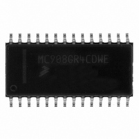
MC908GR4CDWE Freescale Semiconductor, MC908GR4CDWE Datasheet - Page 134

MC908GR4CDWE
Manufacturer Part Number
MC908GR4CDWE
Description
IC MCU 4K FLASH 8MHZ 28-SOIC
Manufacturer
Freescale Semiconductor
Series
HC08r
Specifications of MC908GR4CDWE
Core Processor
HC08
Core Size
8-Bit
Speed
8MHz
Connectivity
SCI, SPI
Peripherals
LVD, POR, PWM
Number Of I /o
17
Program Memory Size
4KB (4K x 8)
Program Memory Type
FLASH
Ram Size
384 x 8
Voltage - Supply (vcc/vdd)
2.7 V ~ 5.5 V
Data Converters
A/D 6x8b
Oscillator Type
Internal
Operating Temperature
-40°C ~ 85°C
Package / Case
28-SOIC (7.5mm Width)
Controller Family/series
HC08
No. Of I/o's
21
Ram Memory Size
384Byte
Cpu Speed
8MHz
No. Of Timers
1
Embedded Interface Type
I2C, SCI, SPI
Rohs Compliant
Yes
Processor Series
HC08GR
Core
HC08
Data Bus Width
8 bit
Data Ram Size
384 B
Interface Type
SCI, SPI
Maximum Clock Frequency
8.2 MHz
Number Of Programmable I/os
21
Number Of Timers
3
Maximum Operating Temperature
+ 85 C
Mounting Style
SMD/SMT
Development Tools By Supplier
FSICEBASE, DEMO908GZ60E, M68CBL05CE, M68EML08GPGTE
Minimum Operating Temperature
- 40 C
On-chip Adc
8 bit, 6 Channel
Lead Free Status / RoHS Status
Lead free / RoHS Compliant
Eeprom Size
-
Lead Free Status / Rohs Status
Details
- Current page: 134 of 286
- Download datasheet (4Mb)
Monitor ROM (MON)
Figure 15-2
1 x V
of 9600, as the internal bus frequency is automatically set to the external frequency divided by four.
Enter monitor mode with pin configuration shown in
rising edge of RST latches monitor mode. Once monitor mode is latched, the values on the specified pins
can change.
Once out of reset, the MCU waits for the host to send eight security bytes. (See Security.) After the
security bytes, the MCU sends a break signal (10 consecutive logic 0s) to the host, indicating that it is
ready to receive a command.
134
V
GND
GND
V
V
GND
V
IRQ
1. External clock is derived by a 32.768 kHz crystal or a 9.8304 MHz off-chip oscillator
2. PTA0 = 1 if serial communication; PTA0 = X if parallel communication
3. PTA1 = 0 → serial, PTA1 = 1 → parallel communication for security code entry
4. DNA = does not apply, X = don’t care
TST
or
X
or
DD
DD
DD
DD
RESET
GND
V
V
V
V
V
V
V
voltage is applied to the IRQ pin. An external oscillator of 9.8304 MHz is required for a baud rate
or
or
TST
TST
TST
DD
DD
DD
DD
shows a simplified diagram of the monitor mode entry when the reset vector is blank and just
$FFFE/
$FFFF
$FFFF
$FFFF
$FFFF
$FFFF
The PTA1 pin must remain at logic 0 for 24 bus cycles after the RST pin
goes high to enter monitor mode properly.
Not
X
X
Table 15-1. Monitor Mode Signal Requirements and Options
OFF
OFF
OFF
OFF
PLL PTB0 PTB1
ON
X
MC68HC908GR8 • MC68HC908GR4 Data Sheet, Rev. 7
X
X
X
X
X
1
X
X
X
X
X
0
External
Clock
9.8304
9.8304
32.768
MHz
MHz
kHz
X
X
X
(1)
CGMOUT
4.9152
4.9152
4.9152
MHz
MHz
MHz
NOTE
—
—
0
Figure 15-1
2.4576
2.4576
2.4576
Freq
MHz
MHz
MHz
Bus
—
—
0
Disabled
Disabled
Disabled
Disabled
Enabled
Enabled
COP
by pulling RST low and then high. The
PTA0 PTA1
X
X
X
X
X
X
1
1
1
Communication
For Serial
X
X
X
0
1
0
1
0
1
Rate
Freescale Semiconductor
Baud
9600
9600
9600
DNA
DNA
DNA
—
—
0
(2) (3)
frequency always
PTB0 and PTB1
until reset goes
illegal address
voltages only
monitor code
encounter an
No operation
PLL enabled
(BCS set) in
mode — will
divided by 4
IRQ = V
Enters user
user mode
Comment
required if
External
Enters
reset
high
TST
Related parts for MC908GR4CDWE
Image
Part Number
Description
Manufacturer
Datasheet
Request
R
Part Number:
Description:
Manufacturer:
Freescale Semiconductor, Inc
Datasheet:
Part Number:
Description:
Manufacturer:
Freescale Semiconductor, Inc
Datasheet:
Part Number:
Description:
Manufacturer:
Freescale Semiconductor, Inc
Datasheet:
Part Number:
Description:
Manufacturer:
Freescale Semiconductor, Inc
Datasheet:
Part Number:
Description:
Manufacturer:
Freescale Semiconductor, Inc
Datasheet:
Part Number:
Description:
Manufacturer:
Freescale Semiconductor, Inc
Datasheet:
Part Number:
Description:
Manufacturer:
Freescale Semiconductor, Inc
Datasheet:
Part Number:
Description:
Manufacturer:
Freescale Semiconductor, Inc
Datasheet:
Part Number:
Description:
Manufacturer:
Freescale Semiconductor, Inc
Datasheet:
Part Number:
Description:
Manufacturer:
Freescale Semiconductor, Inc
Datasheet:
Part Number:
Description:
Manufacturer:
Freescale Semiconductor, Inc
Datasheet:
Part Number:
Description:
Manufacturer:
Freescale Semiconductor, Inc
Datasheet:
Part Number:
Description:
Manufacturer:
Freescale Semiconductor, Inc
Datasheet:
Part Number:
Description:
Manufacturer:
Freescale Semiconductor, Inc
Datasheet:
Part Number:
Description:
Manufacturer:
Freescale Semiconductor, Inc
Datasheet:


