MC908GR4CDWE Freescale Semiconductor, MC908GR4CDWE Datasheet - Page 90
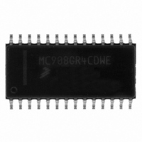
MC908GR4CDWE
Manufacturer Part Number
MC908GR4CDWE
Description
IC MCU 4K FLASH 8MHZ 28-SOIC
Manufacturer
Freescale Semiconductor
Series
HC08r
Specifications of MC908GR4CDWE
Core Processor
HC08
Core Size
8-Bit
Speed
8MHz
Connectivity
SCI, SPI
Peripherals
LVD, POR, PWM
Number Of I /o
17
Program Memory Size
4KB (4K x 8)
Program Memory Type
FLASH
Ram Size
384 x 8
Voltage - Supply (vcc/vdd)
2.7 V ~ 5.5 V
Data Converters
A/D 6x8b
Oscillator Type
Internal
Operating Temperature
-40°C ~ 85°C
Package / Case
28-SOIC (7.5mm Width)
Controller Family/series
HC08
No. Of I/o's
21
Ram Memory Size
384Byte
Cpu Speed
8MHz
No. Of Timers
1
Embedded Interface Type
I2C, SCI, SPI
Rohs Compliant
Yes
Processor Series
HC08GR
Core
HC08
Data Bus Width
8 bit
Data Ram Size
384 B
Interface Type
SCI, SPI
Maximum Clock Frequency
8.2 MHz
Number Of Programmable I/os
21
Number Of Timers
3
Maximum Operating Temperature
+ 85 C
Mounting Style
SMD/SMT
Development Tools By Supplier
FSICEBASE, DEMO908GZ60E, M68CBL05CE, M68EML08GPGTE
Minimum Operating Temperature
- 40 C
On-chip Adc
8 bit, 6 Channel
Lead Free Status / RoHS Status
Lead free / RoHS Compliant
Eeprom Size
-
Lead Free Status / Rohs Status
Details


Configuration Register (CONFIG)
OSCSTOPENB— Oscillator Stop Mode Enable Bar Bit
SCIBDSRC — SCI Baud Rate Clock Source Bit
COPRS — COP Rate Select Bit
LVISTOP — LVI Enable in Stop Mode Bit
LVIRSTD — LVI Reset Disable Bit
LVIPWRD — LVI Power Disable Bit
LVI5OR3 — LVI 5V or 3V Operating Mode Bit
SSREC — Short Stop Recovery Bit
90
OSCSTOPENB enables the oscillator to continue operating during stop mode. Setting the
OSCSTOPENB bit allows the oscillator to operate continuously even during stop mode. This is useful
for driving the timebase module to allow it to generate periodic wakeup while in stop mode. (See Clock
Generator Module (CGM) subsection Stop Mode.)
SCIBDSRC controls the clock source used for the SCI. The setting of this bit affects the frequency at
which the SCI operates.
COPRS selects the COP timeout period. Reset clears COPRS. See
Properly
When the LVIPWRD bit is clear, setting the LVISTOP bit enables the LVI to operate during stop mode.
Reset clears LVISTOP. See Stop Mode.
LVIRSTD disables the reset signal from the LVI module. See
LVIPWRD disables the LVI module. See
LVI5OR3 selects the voltage operating mode of the LVI module. See
(LVI). The voltage mode selected for the LVI should match the operating V
Electrical Specifications
1 = Oscillator enabled to operate during stop mode
0 = Oscillator disabled during stop mode (default)
1 = Internal data bus clock used as clock source for SCI
0 = External oscillator used as clock source for SCI
1 = COP timeout period = 8176 CGMXCLK cycles
0 = COP timeout period = 262,128 CGMXCLK cycles
1 = LVI enabled during stop mode
0 = LVI disabled during stop mode
1 = LVI module resets disabled
0 = LVI module resets enabled
1 = LVI module power disabled
0 = LVI module power enabled
1 = LVI operates in 5V mode.
0 = LVI operates in 3V mode.
(COP).
Note: LVI5OR3 bit is only reset via POR (power-on reset)
Address:
Reset:
Read:
Write:
COPRS
$001F
Bit 7
0
Figure 8-2. Configuration Register 1 (CONFIG1)
for the LVI’s voltage trip points for each of the modes.
MC68HC908GR8 • MC68HC908GR4 Data Sheet, Rev. 7
LVISTOP
6
0
LVIRSTD
5
0
Chapter 14 Low-Voltage Inhibit
LVIPWRD
4
0
LVI5OR3
See Note
3
Chapter 14 Low-Voltage Inhibit
SSREC
2
0
Chapter 9 Computer Operating
Chapter 14 Low-Voltage Inhibit
(LVI).
STOP
DD
1
0
. See
Freescale Semiconductor
COPD
Bit 0
Chapter 23
0
(LVI).
Related parts for MC908GR4CDWE
Image
Part Number
Description
Manufacturer
Datasheet
Request
R

Part Number:
Description:
Manufacturer:
Freescale Semiconductor, Inc
Datasheet:
Part Number:
Description:
Manufacturer:
Freescale Semiconductor, Inc
Datasheet:
Part Number:
Description:
Manufacturer:
Freescale Semiconductor, Inc
Datasheet:
Part Number:
Description:
Manufacturer:
Freescale Semiconductor, Inc
Datasheet:
Part Number:
Description:
Manufacturer:
Freescale Semiconductor, Inc
Datasheet:
Part Number:
Description:
Manufacturer:
Freescale Semiconductor, Inc
Datasheet:
Part Number:
Description:
Manufacturer:
Freescale Semiconductor, Inc
Datasheet:
Part Number:
Description:
Manufacturer:
Freescale Semiconductor, Inc
Datasheet:
Part Number:
Description:
Manufacturer:
Freescale Semiconductor, Inc
Datasheet:
Part Number:
Description:
Manufacturer:
Freescale Semiconductor, Inc
Datasheet:
Part Number:
Description:
Manufacturer:
Freescale Semiconductor, Inc
Datasheet:
Part Number:
Description:
Manufacturer:
Freescale Semiconductor, Inc
Datasheet:
Part Number:
Description:
Manufacturer:
Freescale Semiconductor, Inc
Datasheet:
Part Number:
Description:
Manufacturer:
Freescale Semiconductor, Inc
Datasheet:
Part Number:
Description:
Manufacturer:
Freescale Semiconductor, Inc
Datasheet: