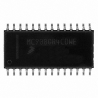
MC908GR4CDWE Freescale Semiconductor, MC908GR4CDWE Datasheet - Page 60

MC908GR4CDWE
Manufacturer Part Number
MC908GR4CDWE
Description
IC MCU 4K FLASH 8MHZ 28-SOIC
Manufacturer
Freescale Semiconductor
Series
HC08r
Specifications of MC908GR4CDWE
Core Processor
HC08
Core Size
8-Bit
Speed
8MHz
Connectivity
SCI, SPI
Peripherals
LVD, POR, PWM
Number Of I /o
17
Program Memory Size
4KB (4K x 8)
Program Memory Type
FLASH
Ram Size
384 x 8
Voltage - Supply (vcc/vdd)
2.7 V ~ 5.5 V
Data Converters
A/D 6x8b
Oscillator Type
Internal
Operating Temperature
-40°C ~ 85°C
Package / Case
28-SOIC (7.5mm Width)
Controller Family/series
HC08
No. Of I/o's
21
Ram Memory Size
384Byte
Cpu Speed
8MHz
No. Of Timers
1
Embedded Interface Type
I2C, SCI, SPI
Rohs Compliant
Yes
Processor Series
HC08GR
Core
HC08
Data Bus Width
8 bit
Data Ram Size
384 B
Interface Type
SCI, SPI
Maximum Clock Frequency
8.2 MHz
Number Of Programmable I/os
21
Number Of Timers
3
Maximum Operating Temperature
+ 85 C
Mounting Style
SMD/SMT
Development Tools By Supplier
FSICEBASE, DEMO908GZ60E, M68CBL05CE, M68EML08GPGTE
Minimum Operating Temperature
- 40 C
On-chip Adc
8 bit, 6 Channel
Lead Free Status / RoHS Status
Lead free / RoHS Compliant
Eeprom Size
-
Lead Free Status / Rohs Status
Details
- Current page: 60 of 286
- Download datasheet (4Mb)
Analog-to-Digital Converter (ADC)
5.7.2 ADC Data Register
One 8-bit result register, ADC data register (ADR), is provided. This register is updated each time an ADC
conversion completes.
5.7.3 ADC Clock Register
The ADC clock register (ADCLK) selects the clock frequency for the ADC.
ADIV2–ADIV0 — ADC Clock Prescaler Bits
60
ADIV2–ADIV0 form a 3-bit field which selects the divide ratio used by the ADC to generate the internal
ADC clock.
approximately 1 MHz.
Address:
Address:
Table 5-2
Reset:
Reset:
Read:
Read:
Write:
Write:
$0003D
$0003E
ADIV2
X = don’t care
Bit 7
AD7
Bit 7
0
0
shows the available clock configurations. The ADC clock should be set to
ADIV2
0
0
0
0
1
MC68HC908GR8 • MC68HC908GR4 Data Sheet, Rev. 7
Figure 5-4. ADC Clock Register (ADCLK)
= Unimplemented
= Unimplemented
ADIV1
Figure 5-3. ADC Data Register (ADR)
AD6
6
0
6
0
Table 5-2. ADC Clock Divide Ratio
ADIV1
X
0
0
1
1
ADIV0
AD5
5
0
5
0
ADIV0
0
1
0
1
X
ADICLK
AD4
4
0
4
0
ADC input clock ÷ 1
ADC input clock ÷ 2
ADC input clock ÷ 4
ADC input clock ÷ 8
ADC input clock ÷ 16
AD3
3
0
3
0
0
ADC Clock Rate
AD2
2
0
2
0
0
AD1
1
0
1
0
0
Freescale Semiconductor
Bit 0
AD0
Bit 0
0
0
0
Related parts for MC908GR4CDWE
Image
Part Number
Description
Manufacturer
Datasheet
Request
R
Part Number:
Description:
Manufacturer:
Freescale Semiconductor, Inc
Datasheet:
Part Number:
Description:
Manufacturer:
Freescale Semiconductor, Inc
Datasheet:
Part Number:
Description:
Manufacturer:
Freescale Semiconductor, Inc
Datasheet:
Part Number:
Description:
Manufacturer:
Freescale Semiconductor, Inc
Datasheet:
Part Number:
Description:
Manufacturer:
Freescale Semiconductor, Inc
Datasheet:
Part Number:
Description:
Manufacturer:
Freescale Semiconductor, Inc
Datasheet:
Part Number:
Description:
Manufacturer:
Freescale Semiconductor, Inc
Datasheet:
Part Number:
Description:
Manufacturer:
Freescale Semiconductor, Inc
Datasheet:
Part Number:
Description:
Manufacturer:
Freescale Semiconductor, Inc
Datasheet:
Part Number:
Description:
Manufacturer:
Freescale Semiconductor, Inc
Datasheet:
Part Number:
Description:
Manufacturer:
Freescale Semiconductor, Inc
Datasheet:
Part Number:
Description:
Manufacturer:
Freescale Semiconductor, Inc
Datasheet:
Part Number:
Description:
Manufacturer:
Freescale Semiconductor, Inc
Datasheet:
Part Number:
Description:
Manufacturer:
Freescale Semiconductor, Inc
Datasheet:
Part Number:
Description:
Manufacturer:
Freescale Semiconductor, Inc
Datasheet:


