MC908GR4CDWE Freescale Semiconductor, MC908GR4CDWE Datasheet - Page 227
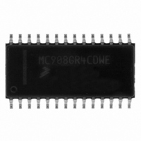
MC908GR4CDWE
Manufacturer Part Number
MC908GR4CDWE
Description
IC MCU 4K FLASH 8MHZ 28-SOIC
Manufacturer
Freescale Semiconductor
Series
HC08r
Specifications of MC908GR4CDWE
Core Processor
HC08
Core Size
8-Bit
Speed
8MHz
Connectivity
SCI, SPI
Peripherals
LVD, POR, PWM
Number Of I /o
17
Program Memory Size
4KB (4K x 8)
Program Memory Type
FLASH
Ram Size
384 x 8
Voltage - Supply (vcc/vdd)
2.7 V ~ 5.5 V
Data Converters
A/D 6x8b
Oscillator Type
Internal
Operating Temperature
-40°C ~ 85°C
Package / Case
28-SOIC (7.5mm Width)
Controller Family/series
HC08
No. Of I/o's
21
Ram Memory Size
384Byte
Cpu Speed
8MHz
No. Of Timers
1
Embedded Interface Type
I2C, SCI, SPI
Rohs Compliant
Yes
Processor Series
HC08GR
Core
HC08
Data Bus Width
8 bit
Data Ram Size
384 B
Interface Type
SCI, SPI
Maximum Clock Frequency
8.2 MHz
Number Of Programmable I/os
21
Number Of Timers
3
Maximum Operating Temperature
+ 85 C
Mounting Style
SMD/SMT
Development Tools By Supplier
FSICEBASE, DEMO908GZ60E, M68CBL05CE, M68EML08GPGTE
Minimum Operating Temperature
- 40 C
On-chip Adc
8 bit, 6 Channel
Lead Free Status / RoHS Status
Lead free / RoHS Compliant
Eeprom Size
-
Lead Free Status / Rohs Status
Details


If the timebase functions are not required during stop mode, reduce the power consumption by stopping
the timebase before enabling the STOP instruction.
21.6 Timebase Register Description
The timebase has one register, the TBCR, which is used to enable the timebase interrupts and set the
rate.
TBIF — Timebase Interrupt Flag
TBR2:TBR0 — Timebase Rate Selection
TACK— Timebase ACKnowledge
Freescale Semiconductor
This read-only flag bit is set when the timebase counter has rolled over.
These read/write bits are used to select the rate of timebase interrupts as shown in
The TACK bit is a write-only bit and always reads as 0. Writing a 1 to this bit clears TBIF, the timebase
interrupt flag bit. Writing a 0 to this bit has no effect.
1 = Timebase interrupt pending
0 = Timebase interrupt not pending
1 = Clear timebase interrupt flag
0 = No effect
Address:
Do not change TBR2–TBR0 bits while the timebase is enabled (TBON = 1).
Reset:
TBR2
Read:
Write:
0
0
0
0
1
1
1
1
Table 21-1. Timebase Rate Selection for OSC1 = 32.768 kHz
$001C
TBIF
Bit 7
0
TBR1
Figure 21-2. Timebase Control Register (TBCR)
0
0
1
1
0
0
1
1
MC68HC908GR8 • MC68HC908GR4 Data Sheet, Rev. 7
= Unimplemented
TBR2
6
0
TBR0
0
1
0
1
0
1
0
1
TBR1
5
0
Divider
32,768
8192
2048
NOTE
128
64
32
16
TBR0
8
R
4
0
= Reserved
TACK
3
0
0
1024
2048
4096
Timebase Interrupt Rate
256
512
Hz
16
1
4
TBIE
2
0
Timebase Register Description
TBON
1
0
~0.24
1000
~ 3.9
62.5
~0.5
250
ms
~2
~1
Bit 0
Table
R
0
21-1.
227
Related parts for MC908GR4CDWE
Image
Part Number
Description
Manufacturer
Datasheet
Request
R

Part Number:
Description:
Manufacturer:
Freescale Semiconductor, Inc
Datasheet:
Part Number:
Description:
Manufacturer:
Freescale Semiconductor, Inc
Datasheet:
Part Number:
Description:
Manufacturer:
Freescale Semiconductor, Inc
Datasheet:
Part Number:
Description:
Manufacturer:
Freescale Semiconductor, Inc
Datasheet:
Part Number:
Description:
Manufacturer:
Freescale Semiconductor, Inc
Datasheet:
Part Number:
Description:
Manufacturer:
Freescale Semiconductor, Inc
Datasheet:
Part Number:
Description:
Manufacturer:
Freescale Semiconductor, Inc
Datasheet:
Part Number:
Description:
Manufacturer:
Freescale Semiconductor, Inc
Datasheet:
Part Number:
Description:
Manufacturer:
Freescale Semiconductor, Inc
Datasheet:
Part Number:
Description:
Manufacturer:
Freescale Semiconductor, Inc
Datasheet:
Part Number:
Description:
Manufacturer:
Freescale Semiconductor, Inc
Datasheet:
Part Number:
Description:
Manufacturer:
Freescale Semiconductor, Inc
Datasheet:
Part Number:
Description:
Manufacturer:
Freescale Semiconductor, Inc
Datasheet:
Part Number:
Description:
Manufacturer:
Freescale Semiconductor, Inc
Datasheet:
Part Number:
Description:
Manufacturer:
Freescale Semiconductor, Inc
Datasheet: