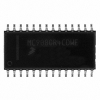
MC908GR4CDWE Freescale Semiconductor, MC908GR4CDWE Datasheet - Page 183

MC908GR4CDWE
Manufacturer Part Number
MC908GR4CDWE
Description
IC MCU 4K FLASH 8MHZ 28-SOIC
Manufacturer
Freescale Semiconductor
Series
HC08r
Specifications of MC908GR4CDWE
Core Processor
HC08
Core Size
8-Bit
Speed
8MHz
Connectivity
SCI, SPI
Peripherals
LVD, POR, PWM
Number Of I /o
17
Program Memory Size
4KB (4K x 8)
Program Memory Type
FLASH
Ram Size
384 x 8
Voltage - Supply (vcc/vdd)
2.7 V ~ 5.5 V
Data Converters
A/D 6x8b
Oscillator Type
Internal
Operating Temperature
-40°C ~ 85°C
Package / Case
28-SOIC (7.5mm Width)
Controller Family/series
HC08
No. Of I/o's
21
Ram Memory Size
384Byte
Cpu Speed
8MHz
No. Of Timers
1
Embedded Interface Type
I2C, SCI, SPI
Rohs Compliant
Yes
Processor Series
HC08GR
Core
HC08
Data Bus Width
8 bit
Data Ram Size
384 B
Interface Type
SCI, SPI
Maximum Clock Frequency
8.2 MHz
Number Of Programmable I/os
21
Number Of Timers
3
Maximum Operating Temperature
+ 85 C
Mounting Style
SMD/SMT
Development Tools By Supplier
FSICEBASE, DEMO908GZ60E, M68CBL05CE, M68EML08GPGTE
Minimum Operating Temperature
- 40 C
On-chip Adc
8 bit, 6 Channel
Lead Free Status / RoHS Status
Lead free / RoHS Compliant
Eeprom Size
-
Lead Free Status / Rohs Status
Details
- Current page: 183 of 286
- Download datasheet (4Mb)
RPF — Reception in Progress Flag Bit
18.8.6 SCI Data Register
The SCI data register (SCDR) is the buffer between the internal data bus and the receive and transmit
shift registers. Reset has no effect on data in the SCI data register.
R7/T7–R0/T0 — Receive/Transmit Data Bits
18.8.7 SCI Baud Rate Register
The baud rate register (SCBR) selects the baud rate for both the receiver and the transmitter.
Freescale Semiconductor
This read-only bit is set when the receiver detects a 0 during the RT1 time period of the start bit search.
RPF does not generate an interrupt request. RPF is reset after the receiver detects false start bits
(usually from noise or a baud rate mismatch) or when the receiver detects an idle character. Polling
RPF before disabling the SCI module or entering stop mode can show whether a reception is in
progress.
Reading address $0018 accesses the read-only received data bits, R7:R0. Writing to address $0018
writes the data to be transmitted, T7:T0. Reset has no effect on the SCI data register.
1 = Reception in progress
0 = No reception in progress
Address:
Address:
Do not use read/modify/write instructions on the SCI data register.
Reset:
Reset:
Read:
Read:
Write:
Write:
$0018
$0019
Bit 7
Bit 7
R7
T7
0
0
Figure 18-16. SCI Baud Rate Register (SCBR)
MC68HC908GR8 • MC68HC908GR4 Data Sheet, Rev. 7
= Unimplemented
Figure 18-15. SCI Data Register (SCDR)
R6
T6
6
6
0
0
SCP1
R5
T5
5
5
0
NOTE
Unaffected by reset
SCP0
R4
T4
4
4
0
R3
T3
R
R
3
3
0
= Reserved
SCR2
R2
T2
2
2
0
SCR1
R1
T1
1
1
0
SCR0
Bit 0
Bit 0
R0
T0
0
I/O Registers
183
Related parts for MC908GR4CDWE
Image
Part Number
Description
Manufacturer
Datasheet
Request
R
Part Number:
Description:
Manufacturer:
Freescale Semiconductor, Inc
Datasheet:
Part Number:
Description:
Manufacturer:
Freescale Semiconductor, Inc
Datasheet:
Part Number:
Description:
Manufacturer:
Freescale Semiconductor, Inc
Datasheet:
Part Number:
Description:
Manufacturer:
Freescale Semiconductor, Inc
Datasheet:
Part Number:
Description:
Manufacturer:
Freescale Semiconductor, Inc
Datasheet:
Part Number:
Description:
Manufacturer:
Freescale Semiconductor, Inc
Datasheet:
Part Number:
Description:
Manufacturer:
Freescale Semiconductor, Inc
Datasheet:
Part Number:
Description:
Manufacturer:
Freescale Semiconductor, Inc
Datasheet:
Part Number:
Description:
Manufacturer:
Freescale Semiconductor, Inc
Datasheet:
Part Number:
Description:
Manufacturer:
Freescale Semiconductor, Inc
Datasheet:
Part Number:
Description:
Manufacturer:
Freescale Semiconductor, Inc
Datasheet:
Part Number:
Description:
Manufacturer:
Freescale Semiconductor, Inc
Datasheet:
Part Number:
Description:
Manufacturer:
Freescale Semiconductor, Inc
Datasheet:
Part Number:
Description:
Manufacturer:
Freescale Semiconductor, Inc
Datasheet:
Part Number:
Description:
Manufacturer:
Freescale Semiconductor, Inc
Datasheet:


