MC908GR4CDWE Freescale Semiconductor, MC908GR4CDWE Datasheet - Page 78
MC908GR4CDWE
Manufacturer Part Number
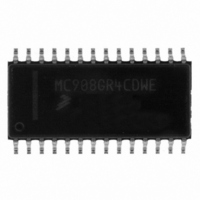
MC908GR4CDWE
Description
IC MCU 4K FLASH 8MHZ 28-SOIC
Manufacturer
Freescale Semiconductor
Series
HC08r
Specifications of MC908GR4CDWE
Core Processor
HC08
Core Size
8-Bit
Speed
8MHz
Connectivity
SCI, SPI
Peripherals
LVD, POR, PWM
Number Of I /o
17
Program Memory Size
4KB (4K x 8)
Program Memory Type
FLASH
Ram Size
384 x 8
Voltage - Supply (vcc/vdd)
2.7 V ~ 5.5 V
Data Converters
A/D 6x8b
Oscillator Type
Internal
Operating Temperature
-40°C ~ 85°C
Package / Case
28-SOIC (7.5mm Width)
Controller Family/series
HC08
No. Of I/o's
21
Ram Memory Size
384Byte
Cpu Speed
8MHz
No. Of Timers
1
Embedded Interface Type
I2C, SCI, SPI
Rohs Compliant
Yes
Processor Series
HC08GR
Core
HC08
Data Bus Width
8 bit
Data Ram Size
384 B
Interface Type
SCI, SPI
Maximum Clock Frequency
8.2 MHz
Number Of Programmable I/os
21
Number Of Timers
3
Maximum Operating Temperature
+ 85 C
Mounting Style
SMD/SMT
Development Tools By Supplier
FSICEBASE, DEMO908GZ60E, M68CBL05CE, M68EML08GPGTE
Minimum Operating Temperature
- 40 C
On-chip Adc
8 bit, 6 Channel
Lead Free Status / RoHS Status
Lead free / RoHS Compliant
Eeprom Size
-
Lead Free Status / Rohs Status
Details


Clock Generator Module (CGMC)
7.4.4 PLL Analog Power Pin (V
V
potential as the V
7.4.5 PLL Analog Ground Pin (V
V
potential as the V
7.4.6 Oscillator Enable Signal (SIMOSCEN)
The SIMOSCEN signal comes from the system integration module (SIM) and enables the oscillator and
PLL.
7.4.7 Oscillator Stop Mode Enable Bit (OSCSTOPENB)
OSCSTOPENB is a bit in the CONFIG register that enables the oscillator to continue operating during
stop mode. If this bit is set, the Oscillator continues running during stop mode. If this bit is not set (default),
the oscillator is controlled by the SIMOSCEN signal which will disable the oscillator during stop mode.
7.4.8 Crystal Output Frequency Signal (CGMXCLK)
CGMXCLK is the crystal oscillator output signal. It runs at the full speed of the crystal (f
directly from the crystal oscillator circuit.
and OSC2 and may not represent the actual circuitry. The duty cycle of CGMXCLK is unknown and may
depend on the crystal and other external factors. Also, the frequency and amplitude of CGMXCLK can be
unstable at startup.
7.4.9 CGMC Base Clock Output (CGMOUT)
CGMOUT is the clock output of the CGMC. This signal goes to the SIM, which generates the MCU clocks.
CGMOUT is a 50 percent duty cycle clock running at twice the bus frequency. CGMOUT is software
programmable to be either the oscillator output, CGMXCLK, divided by two or the VCO clock, CGMVCLK,
divided by two.
7.4.10 CGMC CPU Interrupt (CGMINT)
CGMINT is the interrupt signal generated by the PLL lock detector.
78
DDA
SSA
is a ground pin used by the analog portions of the PLL. Connect the V
is a power pin used by the analog portions of the PLL. Connect the V
Route V
capacitors as close as possible to the package.
Route V
capacitors as close as possible to the package.
DD
SS
pin.
pin.
DDA
SSA
carefully for maximum noise immunity and place bypass
carefully for maximum noise immunity and place bypass
MC68HC908GR8 • MC68HC908GR4 Data Sheet, Rev. 7
DDA
SSA
Figure 7-2
)
)
NOTE
NOTE
shows only the logical relation of CGMXCLK to OSC1
DDA
SSA
pin to the same voltage
pin to the same voltage
Freescale Semiconductor
XCLK
) and comes
Related parts for MC908GR4CDWE
Image
Part Number
Description
Manufacturer
Datasheet
Request
R

Part Number:
Description:
Manufacturer:
Freescale Semiconductor, Inc
Datasheet:
Part Number:
Description:
Manufacturer:
Freescale Semiconductor, Inc
Datasheet:
Part Number:
Description:
Manufacturer:
Freescale Semiconductor, Inc
Datasheet:
Part Number:
Description:
Manufacturer:
Freescale Semiconductor, Inc
Datasheet:
Part Number:
Description:
Manufacturer:
Freescale Semiconductor, Inc
Datasheet:
Part Number:
Description:
Manufacturer:
Freescale Semiconductor, Inc
Datasheet:
Part Number:
Description:
Manufacturer:
Freescale Semiconductor, Inc
Datasheet:
Part Number:
Description:
Manufacturer:
Freescale Semiconductor, Inc
Datasheet:
Part Number:
Description:
Manufacturer:
Freescale Semiconductor, Inc
Datasheet:
Part Number:
Description:
Manufacturer:
Freescale Semiconductor, Inc
Datasheet:
Part Number:
Description:
Manufacturer:
Freescale Semiconductor, Inc
Datasheet:
Part Number:
Description:
Manufacturer:
Freescale Semiconductor, Inc
Datasheet:
Part Number:
Description:
Manufacturer:
Freescale Semiconductor, Inc
Datasheet:
Part Number:
Description:
Manufacturer:
Freescale Semiconductor, Inc
Datasheet:
Part Number:
Description:
Manufacturer:
Freescale Semiconductor, Inc
Datasheet: