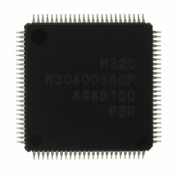
M30800SAGP#U5 Renesas Electronics America, M30800SAGP#U5 Datasheet - Page 241

M30800SAGP#U5
Manufacturer Part Number
M30800SAGP#U5
Description
IC M32C/80 MCU ROMLESS 100LQFP
Manufacturer
Renesas Electronics America
Series
M16C™ M32C/80r
Datasheet
1.M30800SAGP-BLU5.pdf
(354 pages)
Specifications of M30800SAGP#U5
Core Processor
M16C/80
Core Size
16-Bit
Speed
20MHz
Connectivity
I²C, IEBus, SIO, UART/USART
Peripherals
DMA, WDT
Number Of I /o
45
Program Memory Type
ROMless
Ram Size
8K x 8
Voltage - Supply (vcc/vdd)
3 V ~ 5.5 V
Data Converters
A/D 10x10b, D/A 2x8b
Oscillator Type
Internal
Operating Temperature
-20°C ~ 85°C
Package / Case
100-LQFP
For Use With
R0K330879S001BE - KIT DEV RSK M32C/87R0K330879S000BE - KIT DEV RSK M32C/87
Lead Free Status / RoHS Status
Lead free / RoHS Compliant
Eeprom Size
-
Program Memory Size
-
Available stocks
Company
Part Number
Manufacturer
Quantity
Price
Part Number:
M30800SAGP#U5M30800SAGP#D3
Manufacturer:
Renesas Electronics America
Quantity:
10 000
- Current page: 241 of 354
- Download datasheet (3Mb)
M
R
R
17. A/D Converter
e
E
3
. v
J
2
Table 17.1 A/D Converter Specifications
NOTES:
0
A/D Conversion Method
Analog Input Voltage
Operating Clock, Ø
Resolution
Operating Mode
Analog Input Pins
A/D Conversion Start Condition
Conversion Rate Per Pin
C
The A/D converter consists of one 10-bit successive approximation A/D converter with a capacitive cou-
pling amplifier.
The result of an A/D conversion is stored into the A/D registers corresponding to selected pins. It is stored
into the AD00 register only when DMAC operating mode is entered.
Table 17.1 lists specifications of the A/D converter. Figure 17.1 shows a block diagram of the
A/D converter. Figures 17.2 to 17.6 show registers associated with the A/D converter.
1
9
1. Analog input voltage is not affected by the sample and hold function status.
2. Ø
3. AV
0 .
8 /
B
0
0
0
Ø
Without the sample and hold function, the Ø
With the sample and hold function, the Ø
2
AD
AD
7
G
N
CC
1
o
o r
0 -
frequency must be under 16 MHz when V
frequency must be under 10 MHz when V
. v
=V
u
1
p
0
0
REF
Item
, 1
0
2
=V
0
(3)
0
AD (2)
CC1
5
(1)
Page 220
, A/D input voltage (for AN
f o
Successive approximation (with a capacitive coupling amplifier)
0V to AV
f
8 bits or 10 bits
One-shot mode, repeat mode, single sweep mode, repeat sweep mode 0,
repeat sweep mode 1
10 pins
• Software trigger
• External trigger (re-trigger is enabled)
• Hardware trigger (re-trigger is enabled)
• Without the sample and hold function
• With the sample and hold function
AD
When a falling edge is applied to the AD
The timer B2 interrupt request of the three-phase motor control timer functions
3
8 pins for AN
2 extended input pins (ANEX0 and ANEX1)
The ADST bit in the AD0CON0 register is set to "1" (A/D conversion started) by
program
program
(after the ICTB2 counter completes counting) is generated after the ADST bit is
set to "1" by program
3
8-bit resolution : 49 Ø
10-bit resolution : 59 Ø
8-bit resolution : 28 Ø
10-bit resolution : 33 Ø
, f
0
AD
/2, f
CC
AD
AD
(V
/3, f
AD
frequency is 1 MHz or more.
CC1
0
0
to AN
CC1
CC1
to AN
frequency is 250 kHz or more.
AD
)
/4, f
=5V.
=3.3V.
7
7
, ANEX0, and ANEX1)
AD
AD
AD
AD
AD
/6, f
cycles
cycles
cycles
cycles
AD
Specification
/8
__________
TRG
pin after the ADST bit is set to "1" by
V
CC1
.
17. A/D Converter
Related parts for M30800SAGP#U5
Image
Part Number
Description
Manufacturer
Datasheet
Request
R

Part Number:
Description:
KIT STARTER FOR M16C/29
Manufacturer:
Renesas Electronics America
Datasheet:

Part Number:
Description:
KIT STARTER FOR R8C/2D
Manufacturer:
Renesas Electronics America
Datasheet:

Part Number:
Description:
R0K33062P STARTER KIT
Manufacturer:
Renesas Electronics America
Datasheet:

Part Number:
Description:
KIT STARTER FOR R8C/23 E8A
Manufacturer:
Renesas Electronics America
Datasheet:

Part Number:
Description:
KIT STARTER FOR R8C/25
Manufacturer:
Renesas Electronics America
Datasheet:

Part Number:
Description:
KIT STARTER H8S2456 SHARPE DSPLY
Manufacturer:
Renesas Electronics America
Datasheet:

Part Number:
Description:
KIT STARTER FOR R8C38C
Manufacturer:
Renesas Electronics America
Datasheet:

Part Number:
Description:
KIT STARTER FOR R8C35C
Manufacturer:
Renesas Electronics America
Datasheet:

Part Number:
Description:
KIT STARTER FOR R8CL3AC+LCD APPS
Manufacturer:
Renesas Electronics America
Datasheet:

Part Number:
Description:
KIT STARTER FOR RX610
Manufacturer:
Renesas Electronics America
Datasheet:

Part Number:
Description:
KIT STARTER FOR R32C/118
Manufacturer:
Renesas Electronics America
Datasheet:

Part Number:
Description:
KIT DEV RSK-R8C/26-29
Manufacturer:
Renesas Electronics America
Datasheet:

Part Number:
Description:
KIT STARTER FOR SH7124
Manufacturer:
Renesas Electronics America
Datasheet:

Part Number:
Description:
KIT STARTER FOR H8SX/1622
Manufacturer:
Renesas Electronics America
Datasheet:

Part Number:
Description:
KIT DEV FOR SH7203
Manufacturer:
Renesas Electronics America
Datasheet:


