DF2367VTE33 Renesas Electronics America, DF2367VTE33 Datasheet - Page 119
DF2367VTE33
Manufacturer Part Number
DF2367VTE33
Description
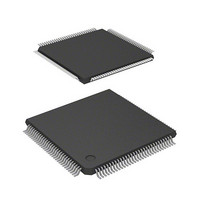
IC H8S MCU FLASH 384K 120TQFP
Manufacturer
Renesas Electronics America
Series
H8® H8S/2300r
Specifications of DF2367VTE33
Core Processor
H8S/2000
Core Size
16-Bit
Speed
33MHz
Connectivity
I²C, IrDA, SCI, SmartCard
Peripherals
DMA, POR, PWM, WDT
Number Of I /o
84
Program Memory Size
384KB (384K x 8)
Program Memory Type
FLASH
Ram Size
24K x 8
Voltage - Supply (vcc/vdd)
3 V ~ 3.6 V
Data Converters
A/D 10x10b, D/A 2x8b
Oscillator Type
Internal
Operating Temperature
-20°C ~ 75°C
Package / Case
120-TQFP, 120-VQFP
Lead Free Status / RoHS Status
Contains lead / RoHS non-compliant
Eeprom Size
-
Other names
HD64F2367VTE33
HD64F2367VTE33
HD64F2367VTE33
Available stocks
Company
Part Number
Manufacturer
Quantity
Price
Company:

Part Number:
DF2367VTE33V
Manufacturer:
Renesas Electronics America
Quantity:
10 000


Bit
7, 6
5, 4
3
2
1
0
Bit Name
−
−
FLSHE
−
EXPE
RAME
Initial Value
All 1
All 0
0
0
−
1
R/W
R/W
R/W
R/W
R/W
R/W
−
R/W
R/W
Descriptions
Reserved
The initial value should not be modified.
Reserved
The initial value should not be modified.
Flash Memory Control Register Enable
Controls CPU access to the flash memory control
registers (FLMCR1, FLMCR2, EBR1, and EBR2). If
this bit is set to 1, the flash memory control registers
can be read/written to. If this bit is cleared to 0, the
flash memory control registers are not selected. At
this time, the contents of the flash memory control
registers are maintained. This bit should be written
to 0 in other than flash memory version.
0: Flash memory control registers are not selected
1: Flash memory control registers are selected for
Reserved
This bit is always read as 0 and cannot be modified.
External Bus Mode Enable
Sets external bus mode.
In modes 1, 2, and 4, this bit is fixed at 1 and cannot
be modified. In mode 3 and 7, this bit has an initial
value of 0, and can be read and written.
Writing of 0 to EXPE when its value is 1 should only
be carried out when an external bus cycle is not
being executed.
0: External bus disabled
1: External bus enabled
RAM Enable
Enables or disables the on-chip RAM. The RAME
bit is initialized when the reset status is released.
0: On-chip RAM is disabled
1: On-chip RAM is enabled
for area H'FFFFC8 to H'FFFFCB
area H'FFFFC8 to H'FFFFCB
Rev.6.00 Mar. 18, 2009 Page 59 of 980
Section 3 MCU Operating Modes
REJ09B0050-0600
Related parts for DF2367VTE33
Image
Part Number
Description
Manufacturer
Datasheet
Request
R

Part Number:
Description:
CONN PLUG 12POS DUAL 0.5MM SMD
Manufacturer:
Hirose Electric Co Ltd
Datasheet:
Part Number:
Description:
CONN PLUG 18POS DUAL 0.5MM SMD
Manufacturer:
Hirose Electric Co Ltd
Datasheet:
Part Number:
Description:
CONN PLUG 14POS DUAL 0.5MM SMD
Manufacturer:
Hirose Electric Co Ltd
Datasheet:
Part Number:
Description:
CONN RECEPT 20POS DUAL 0.5MM SMD
Manufacturer:
Hirose Electric Co Ltd
Datasheet:
Part Number:
Description:
CONN PLUG 16POS DUAL 0.5MM SMD
Manufacturer:
Hirose Electric Co Ltd
Datasheet:
Part Number:
Description:
CONN RECEPT 16POS DUAL 0.5MM SMD
Manufacturer:
Hirose Electric Co Ltd
Datasheet:
Part Number:
Description:
CONN PLUG 20POS DUAL 0.5MM SMD
Manufacturer:
Hirose Electric Co Ltd
Datasheet:
Part Number:
Description:
CONN PLUG 30POS DUAL 0.5MM SMD
Manufacturer:
Hirose Electric Co Ltd
Datasheet:
Part Number:
Description:
CONN RECEPT 30POS DUAL 0.5MM SMD
Manufacturer:
Hirose Electric Co Ltd
Datasheet:
Part Number:
Description:
CONN PLUG 40POS DUAL 0.5MM SMD
Manufacturer:
Hirose Electric Co Ltd
Datasheet:

Part Number:
Description:
KIT STARTER FOR M16C/29
Manufacturer:
Renesas Electronics America
Datasheet:

Part Number:
Description:
KIT STARTER FOR R8C/2D
Manufacturer:
Renesas Electronics America
Datasheet:

Part Number:
Description:
R0K33062P STARTER KIT
Manufacturer:
Renesas Electronics America
Datasheet:

Part Number:
Description:
KIT STARTER FOR R8C/23 E8A
Manufacturer:
Renesas Electronics America
Datasheet:

Part Number:
Description:
KIT STARTER FOR R8C/25
Manufacturer:
Renesas Electronics America
Datasheet: