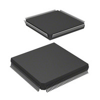
DF2505FC26V Renesas Electronics America, DF2505FC26V Datasheet - Page 205

DF2505FC26V
Manufacturer Part Number
DF2505FC26V
Description
IC H8S/2505 MCU FLASH 144QFP
Manufacturer
Renesas Electronics America
Series
H8® H8S/2500r
Specifications of DF2505FC26V
Core Processor
H8S/2000
Core Size
16-Bit
Speed
26MHz
Connectivity
I²C, SCI
Peripherals
POR, PWM, WDT
Number Of I /o
104
Program Memory Size
384KB (384K x 8)
Program Memory Type
FLASH
Ram Size
32K x 8
Voltage - Supply (vcc/vdd)
3 V ~ 5.5 V
Data Converters
A/D 16x10b; D/A 2x8b
Oscillator Type
Internal
Operating Temperature
-40°C ~ 85°C
Package / Case
144-QFP
Lead Free Status / RoHS Status
Lead free / RoHS Compliant
Eeprom Size
-
- Current page: 205 of 980
- Download datasheet (6Mb)
7.7
With this LSI, external address space of area 0 can be designated as burst ROM space, and burst
ROM interfacing can be performed. The burst ROM space interface enables 16-bit configuration
ROM with burst access capability to be accessed at high speed.
Area 0 can be designated as burst ROM space by means of the BRSTRM bit in BCRH.
Consecutive burst accesses of a maximum of 4 words or 8 words can be performed for CPU
instruction fetches only. One or two states can be selected for burst access.
7.7.1
The number of access states in the initial cycle (full access) of the burst ROM interface is in
accordance with the setting of the AST0 bit in ASTCR. Also, when the AST0 bit is set to 1, wait
states can be inserted. One or two states can be selected for the burst cycle, according to the
setting of the BRSTS1 bit in BCRH. Wait states cannot be inserted. When area 0 is designated as
burst ROM space, it becomes 16-bit access space regardless of the setting of the ABW0 bit in
ABWCR.
When the BRSTS0 bit in BCRH is cleared to 0, burst access of up to 4 words is performed; when
the BRSTS0 bit is set to 1, burst access of up to 8 words is performed.
The basic access timing for burst ROM space is shown in figures 7.25 and 7.26. The timing shown
in figure 7.25 is for the case where the AST0 and BRSTS1 bits are both set to 1, and that in figure
7.26 is for the case where both these bits are cleared to 0.
Burst ROM Interface
Basic Timing
Rev. 6.00 Sep. 24, 2009 Page 157 of 928
Section 7 Bus Controller
REJ09B0099-0600
Related parts for DF2505FC26V
Image
Part Number
Description
Manufacturer
Datasheet
Request
R

Part Number:
Description:
KIT STARTER FOR M16C/29
Manufacturer:
Renesas Electronics America
Datasheet:

Part Number:
Description:
KIT STARTER FOR R8C/2D
Manufacturer:
Renesas Electronics America
Datasheet:

Part Number:
Description:
R0K33062P STARTER KIT
Manufacturer:
Renesas Electronics America
Datasheet:

Part Number:
Description:
KIT STARTER FOR R8C/23 E8A
Manufacturer:
Renesas Electronics America
Datasheet:

Part Number:
Description:
KIT STARTER FOR R8C/25
Manufacturer:
Renesas Electronics America
Datasheet:

Part Number:
Description:
KIT STARTER H8S2456 SHARPE DSPLY
Manufacturer:
Renesas Electronics America
Datasheet:

Part Number:
Description:
KIT STARTER FOR R8C38C
Manufacturer:
Renesas Electronics America
Datasheet:

Part Number:
Description:
KIT STARTER FOR R8C35C
Manufacturer:
Renesas Electronics America
Datasheet:

Part Number:
Description:
KIT STARTER FOR R8CL3AC+LCD APPS
Manufacturer:
Renesas Electronics America
Datasheet:

Part Number:
Description:
KIT STARTER FOR RX610
Manufacturer:
Renesas Electronics America
Datasheet:

Part Number:
Description:
KIT STARTER FOR R32C/118
Manufacturer:
Renesas Electronics America
Datasheet:

Part Number:
Description:
KIT DEV RSK-R8C/26-29
Manufacturer:
Renesas Electronics America
Datasheet:

Part Number:
Description:
KIT STARTER FOR SH7124
Manufacturer:
Renesas Electronics America
Datasheet:

Part Number:
Description:
KIT STARTER FOR H8SX/1622
Manufacturer:
Renesas Electronics America
Datasheet:

Part Number:
Description:
KIT DEV FOR SH7203
Manufacturer:
Renesas Electronics America
Datasheet:


