DF2505FC26V Renesas Electronics America, DF2505FC26V Datasheet - Page 391
DF2505FC26V
Manufacturer Part Number
DF2505FC26V
Description
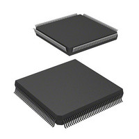
IC H8S/2505 MCU FLASH 144QFP
Manufacturer
Renesas Electronics America
Series
H8® H8S/2500r
Specifications of DF2505FC26V
Core Processor
H8S/2000
Core Size
16-Bit
Speed
26MHz
Connectivity
I²C, SCI
Peripherals
POR, PWM, WDT
Number Of I /o
104
Program Memory Size
384KB (384K x 8)
Program Memory Type
FLASH
Ram Size
32K x 8
Voltage - Supply (vcc/vdd)
3 V ~ 5.5 V
Data Converters
A/D 16x10b; D/A 2x8b
Oscillator Type
Internal
Operating Temperature
-40°C ~ 85°C
Package / Case
144-QFP
Lead Free Status / RoHS Status
Lead free / RoHS Compliant
Eeprom Size
-


10.9
10.9.1
TPU operation can be disabled or enabled using the module stop control register. The initial
setting is for TPU operation to be halted. Register access is enabled by clearing module stop
mode. For details, see section 22, Power-Down Modes.
10.9.2
The input clock pulse width must be at least 1.5 states in the case of single-edge detection, and at
least 2.5 states in the case of both-edge detection. The TPU will not operate properly at narrower
pulse widths.
In phase counting mode, the phase difference and overlap between the two input clocks must be at
least 1.5 states, and the pulse width must be at least 2.5 states. Figure 10.44 shows the input clock
conditions in phase counting mode.
Figure 10.44 Phase Difference, Overlap, and Pulse Width in Phase Counting Mode
TCLKA
(TCLKC)
TCLKB
(TCLKD)
Notes: Phase difference and overlap
Usage Notes
Module Stop Mode Setting
Input Clock Restrictions
Pulse width
Overlap
Pulse width
Phase
differ-
ence
Overlap
: 1.5 states or more
: 2.5 states or more
Phase
differ-
ence
Pulse width
Pulse width
Rev. 6.00 Sep. 24, 2009 Page 343 of 928
Section 10 16-Bit Timer Pulse Unit (TPU)
Pulse width
REJ09B0099-0600
Related parts for DF2505FC26V
Image
Part Number
Description
Manufacturer
Datasheet
Request
R

Part Number:
Description:
KIT STARTER FOR M16C/29
Manufacturer:
Renesas Electronics America
Datasheet:

Part Number:
Description:
KIT STARTER FOR R8C/2D
Manufacturer:
Renesas Electronics America
Datasheet:

Part Number:
Description:
R0K33062P STARTER KIT
Manufacturer:
Renesas Electronics America
Datasheet:

Part Number:
Description:
KIT STARTER FOR R8C/23 E8A
Manufacturer:
Renesas Electronics America
Datasheet:

Part Number:
Description:
KIT STARTER FOR R8C/25
Manufacturer:
Renesas Electronics America
Datasheet:

Part Number:
Description:
KIT STARTER H8S2456 SHARPE DSPLY
Manufacturer:
Renesas Electronics America
Datasheet:

Part Number:
Description:
KIT STARTER FOR R8C38C
Manufacturer:
Renesas Electronics America
Datasheet:

Part Number:
Description:
KIT STARTER FOR R8C35C
Manufacturer:
Renesas Electronics America
Datasheet:

Part Number:
Description:
KIT STARTER FOR R8CL3AC+LCD APPS
Manufacturer:
Renesas Electronics America
Datasheet:
Part Number:
Description:
KIT STARTER FOR RX610
Manufacturer:
Renesas Electronics America
Datasheet:

Part Number:
Description:
KIT STARTER FOR R32C/118
Manufacturer:
Renesas Electronics America
Datasheet:

Part Number:
Description:
KIT DEV RSK-R8C/26-29
Manufacturer:
Renesas Electronics America
Datasheet:

Part Number:
Description:
KIT STARTER FOR SH7124
Manufacturer:
Renesas Electronics America
Datasheet:

Part Number:
Description:
KIT STARTER FOR H8SX/1622
Manufacturer:
Renesas Electronics America
Datasheet:

Part Number:
Description:
KIT DEV FOR SH7203
Manufacturer:
Renesas Electronics America
Datasheet: