DF2505FC26V Renesas Electronics America, DF2505FC26V Datasheet - Page 456
DF2505FC26V
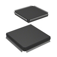
Manufacturer Part Number
DF2505FC26V
Description
IC H8S/2505 MCU FLASH 144QFP
Manufacturer
Renesas Electronics America
Series
H8® H8S/2500r
Specifications of DF2505FC26V
Core Processor
H8S/2000
Core Size
16-Bit
Speed
26MHz
Connectivity
I²C, SCI
Peripherals
POR, PWM, WDT
Number Of I /o
104
Program Memory Size
384KB (384K x 8)
Program Memory Type
FLASH
Ram Size
32K x 8
Voltage - Supply (vcc/vdd)
3 V ~ 5.5 V
Data Converters
A/D 16x10b; D/A 2x8b
Oscillator Type
Internal
Operating Temperature
-40°C ~ 85°C
Package / Case
144-QFP
Lead Free Status / RoHS Status
Lead free / RoHS Compliant
Eeprom Size
-


Section 13 Serial Communication Interface (SCI)
• Smart Card Interface Mode (When SMIF in SCMR Is 1)
Rev. 6.00 Sep. 24, 2009 Page 408 of 928
REJ09B0099-0600
Bit
7
6
5
4
Bit Name
TIE
RIE
TE
RE
Initial
Value
0
0
0
0
R/W
R/W
R/W
R/W
R/W
Description
Transmit Interrupt Enable
When this bit is set to 1, TXI interrupt request is enabled.
TXI interrupt request cancellation can be performed by
reading 1 from the TDRE flag in SSR, then clearing it to
0, or clearing the TIE bit to 0.
Receive Interrupt Enable
When this bit is set to 1, RXI and ERI interrupt requests
are enabled.
RXI and ERI interrupt request cancellation can be
performed by reading 1 from the RDRF, FER, PER, or
ORER flag in SSR, then clearing the flag to 0, or clearing
the RIE bit to 0.
Transmit Enable
When this bit is set to 1, transmission is enabled.
In this state, serial transmission is started when transmit
data is written to TDR and the TDRE flag in SSR is
cleared to 0.
SMR setting must be performed to decide the transfer
format before setting the TE bit to 1. When this bit is
cleared to 0, the transmission operation is disabled, and
the TDRE flag is fixed at 1.
Receive Enable
When this bit is set to 1, reception is enabled.
Serial reception is started in this state when a start bit is
detected in asynchronous mode or serial clock input is
detected in clocked synchronous mode.
SMR setting must be performed to decide the reception
format before setting the RE bit to 1.
Clearing the RE bit to 0 does not affect the RDRF, FER,
PER, and ORER flags, which retain their states.
Related parts for DF2505FC26V
Image
Part Number
Description
Manufacturer
Datasheet
Request
R

Part Number:
Description:
KIT STARTER FOR M16C/29
Manufacturer:
Renesas Electronics America
Datasheet:

Part Number:
Description:
KIT STARTER FOR R8C/2D
Manufacturer:
Renesas Electronics America
Datasheet:

Part Number:
Description:
R0K33062P STARTER KIT
Manufacturer:
Renesas Electronics America
Datasheet:

Part Number:
Description:
KIT STARTER FOR R8C/23 E8A
Manufacturer:
Renesas Electronics America
Datasheet:

Part Number:
Description:
KIT STARTER FOR R8C/25
Manufacturer:
Renesas Electronics America
Datasheet:

Part Number:
Description:
KIT STARTER H8S2456 SHARPE DSPLY
Manufacturer:
Renesas Electronics America
Datasheet:

Part Number:
Description:
KIT STARTER FOR R8C38C
Manufacturer:
Renesas Electronics America
Datasheet:

Part Number:
Description:
KIT STARTER FOR R8C35C
Manufacturer:
Renesas Electronics America
Datasheet:

Part Number:
Description:
KIT STARTER FOR R8CL3AC+LCD APPS
Manufacturer:
Renesas Electronics America
Datasheet:
Part Number:
Description:
KIT STARTER FOR RX610
Manufacturer:
Renesas Electronics America
Datasheet:

Part Number:
Description:
KIT STARTER FOR R32C/118
Manufacturer:
Renesas Electronics America
Datasheet:

Part Number:
Description:
KIT DEV RSK-R8C/26-29
Manufacturer:
Renesas Electronics America
Datasheet:

Part Number:
Description:
KIT STARTER FOR SH7124
Manufacturer:
Renesas Electronics America
Datasheet:

Part Number:
Description:
KIT STARTER FOR H8SX/1622
Manufacturer:
Renesas Electronics America
Datasheet:

Part Number:
Description:
KIT DEV FOR SH7203
Manufacturer:
Renesas Electronics America
Datasheet: