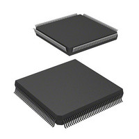
DF2505FC26V Renesas Electronics America, DF2505FC26V Datasheet - Page 786

DF2505FC26V
Manufacturer Part Number
DF2505FC26V
Description
IC H8S/2505 MCU FLASH 144QFP
Manufacturer
Renesas Electronics America
Series
H8® H8S/2500r
Specifications of DF2505FC26V
Core Processor
H8S/2000
Core Size
16-Bit
Speed
26MHz
Connectivity
I²C, SCI
Peripherals
POR, PWM, WDT
Number Of I /o
104
Program Memory Size
384KB (384K x 8)
Program Memory Type
FLASH
Ram Size
32K x 8
Voltage - Supply (vcc/vdd)
3 V ~ 5.5 V
Data Converters
A/D 16x10b; D/A 2x8b
Oscillator Type
Internal
Operating Temperature
-40°C ~ 85°C
Package / Case
144-QFP
Lead Free Status / RoHS Status
Lead free / RoHS Compliant
Eeprom Size
-
- Current page: 786 of 980
- Download datasheet (6Mb)
Section 20 Flash Memory
20.9.4
1. In auto-programming mode, 128-byte simultaneous programming is performed. In this
2. Data transfer of 128 bytes must be performed even in the programming of 128 bytes or less.
3. Lower seven bits of the address to be transferred should be set to low. When an address other
4. The memory address transfer is made in the second cycle. A transfer should not be made in
5. Do not write commands while programming is in progress.
6. One time automatic programming should be performed for each 128-byte block of address.
7. To confirm the end of automatic programming, check the signal on I/O6 pin. Confirmation in
8. Information on the pins I/O6 and I/O7 is retained until the next command is written. As long
For details on the AC characteristics in auto-program mode, see section 20.11, AC Characteristics
and Timing in Programmer Mode.
20.9.5
1. In auto-erase mode, only erasing the entire memory is supported.
2. Command writing should not be preformed during automatic erasing.
3. To confirm the end of automatic erasing, check the signal on the I/O6 pin. Confirmation in
4. Information on the pins I/O6 and I/O7 is retained until the next command is written. As long
For details on AC characteristics in auto-erase mode, see section 20.11, AC Characteristics and
Timing in Programmer Mode.
Rev. 6.00 Sep. 24, 2009 Page 738 of 928
REJ09B0099-0600
process, 128 bytes of data are transferred in succession.
H'FF should be written to those address that are unnecessary written to.
than valid address is input, programming error is occurred, although memory programming
operation is started.
the third cycle or later.
Additional programming of the block to the address where already programmed is not
possible.
status-read mode is also possible. (Status polling of the I/O7 pin is used to check the end
status of automatic programming.)
as no command is written, the information can be read by enabling the CE and OE.
status read mode is also possible. (Status polling of the I/O7 pin is used to check the end
status of automatic erasure.)
as other command is written, the information can be read by enabling the CE and OE.
Auto-Program Mode
Auto-Erase Mode
Related parts for DF2505FC26V
Image
Part Number
Description
Manufacturer
Datasheet
Request
R

Part Number:
Description:
KIT STARTER FOR M16C/29
Manufacturer:
Renesas Electronics America
Datasheet:

Part Number:
Description:
KIT STARTER FOR R8C/2D
Manufacturer:
Renesas Electronics America
Datasheet:

Part Number:
Description:
R0K33062P STARTER KIT
Manufacturer:
Renesas Electronics America
Datasheet:

Part Number:
Description:
KIT STARTER FOR R8C/23 E8A
Manufacturer:
Renesas Electronics America
Datasheet:

Part Number:
Description:
KIT STARTER FOR R8C/25
Manufacturer:
Renesas Electronics America
Datasheet:

Part Number:
Description:
KIT STARTER H8S2456 SHARPE DSPLY
Manufacturer:
Renesas Electronics America
Datasheet:

Part Number:
Description:
KIT STARTER FOR R8C38C
Manufacturer:
Renesas Electronics America
Datasheet:

Part Number:
Description:
KIT STARTER FOR R8C35C
Manufacturer:
Renesas Electronics America
Datasheet:

Part Number:
Description:
KIT STARTER FOR R8CL3AC+LCD APPS
Manufacturer:
Renesas Electronics America
Datasheet:

Part Number:
Description:
KIT STARTER FOR RX610
Manufacturer:
Renesas Electronics America
Datasheet:

Part Number:
Description:
KIT STARTER FOR R32C/118
Manufacturer:
Renesas Electronics America
Datasheet:

Part Number:
Description:
KIT DEV RSK-R8C/26-29
Manufacturer:
Renesas Electronics America
Datasheet:

Part Number:
Description:
KIT STARTER FOR SH7124
Manufacturer:
Renesas Electronics America
Datasheet:

Part Number:
Description:
KIT STARTER FOR H8SX/1622
Manufacturer:
Renesas Electronics America
Datasheet:

Part Number:
Description:
KIT DEV FOR SH7203
Manufacturer:
Renesas Electronics America
Datasheet:


