AT91SAM7S32-AU-001 Atmel, AT91SAM7S32-AU-001 Datasheet - Page 194
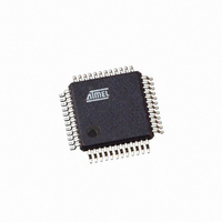
AT91SAM7S32-AU-001
Manufacturer Part Number
AT91SAM7S32-AU-001
Description
IC ARM7 MCU 32BIT 32K 48LQFP
Manufacturer
Atmel
Series
AT91SAMr
Specifications of AT91SAM7S32-AU-001
Core Processor
ARM7
Core Size
16/32-Bit
Speed
55MHz
Connectivity
I²C, SPI, SSC, UART/USART
Peripherals
Brown-out Detect/Reset, POR, PWM, WDT
Number Of I /o
21
Program Memory Size
32KB (32K x 8)
Program Memory Type
FLASH
Ram Size
8K x 8
Voltage - Supply (vcc/vdd)
1.65 V ~ 1.95 V
Data Converters
A/D 8x10b
Oscillator Type
Internal
Operating Temperature
-40°C ~ 85°C
Package / Case
48-LQFP
For Use With
AT91SAM7S-EK - KIT EVAL FOR ARM AT91SAM7S
Lead Free Status / RoHS Status
Lead free / RoHS Compliant
Eeprom Size
-
Other names
AT91SAM7S32-AU001
Available stocks
Company
Part Number
Manufacturer
Quantity
Price


194
AT91SAM7S Series Preliminary
4. Selection of Master Clock and Processor Clock
• If a new value for CSS field corresponds to PLL Clock,
The DIV field is used to control divider itself. A value between 0 and 255 can be pro-
grammed. Divider output is divider input divided by DIV parameter. By default DIV
parameter is set to 0 which means that divider is turned off.
The OUT field is used to select the PLL B output frequency range.
The MUL field is the PLL multiplier factor. This parameter can be programmed between 0
and 2047. If MUL is set to 0, PLL will be turned off, otherwise the PLL output frequency is
PLL input frequency multiplied by (MUL + 1).
The PLLCOUNT field specifies the number of slow clock cycles before LOCK bit is set in the
PMC_SR register after CKGR_PLLR register has been written.
Once the PMC_PLL register has been written, the user must wait for the LOCK bit to be set
in the PMC_SR register. This can be done either by polling the status register or by waiting
the interrupt line to be raised if the associated interrupt to LOCK has been enabled in the
PMC_IER register. All parameters in CKGR_PLLR can be programmed in a single write
operation. If at some stage one of the following parameters, MUL, DIV is modified, LOCK bit
will go low to indicate that PLL is not ready yet. When PLL is locked, LOCK will be set again.
The user is constrained to wait for LOCK bit to be set before using the PLL output clock.
The USBDIV field is used to control the additional divider by 1, 2 or 4, which generates the
USB clock(s) (Does not pertain to AT91SAM7S32/16.)
Code Example:
If PLL and divider are enabled, the PLL input clock is the main clock. PLL output clock is PLL
input clock multiplied by 5. Once CKGR_PLLR has been written, LOCK bit will be set after
eight slow clock cycles.
The Master Clock and the Processor Clock are configurable via the PMC_MCKR register.
The CSS field is used to select the Master Clock divider source. By default, the selected
clock source is slow clock.
The PRES field is used to control the Master Clock prescaler. The user can choose between
different values (1, 2, 4, 8, 16, 32, 64). Master Clock output is prescaler input divided by
PRES parameter. By default, PRES parameter is set to 1 which means that master clock is
equal to slow clock.
Once the PMC_MCKR register has been written, the user must wait for the MCKRDY bit to
be set in the PMC_SR register. This can be done either by polling the status register or by
waiting for the interrupt line to be raised if the associated interrupt to MCKRDY has been
enabled in the PMC_IER register.
The PMC_MCKR register must not be programmed in a single write operation. The pre-
ferred programming sequence for the PMC_MCKR register is as follows:
– Program the PRES field in the PMC_MCKR register.
– Wait for the MCKRDY bit to be set in the PMC_SR register.
write_register(CKGR_PLLR,0x00040805)
6175K–ATARM–30-Aug-10
Related parts for AT91SAM7S32-AU-001
Image
Part Number
Description
Manufacturer
Datasheet
Request
R

Part Number:
Description:
Manufacturer:
ATMEL Corporation
Datasheet:

Part Number:
Description:
AT91 ARM Thumb-based Microcontrollers
Manufacturer:
ATMEL [ATMEL Corporation]
Datasheet:

Part Number:
Description:
IC ARM7 MCU FLASH 32K 48QFN
Manufacturer:
Atmel
Datasheet:

Part Number:
Description:
IC MCU ARM7 32KB FLASH 48LQFP
Manufacturer:
Atmel
Datasheet:
Part Number:
Description:
IC MCU ARM7 32KB FLASH 48-VQFN
Manufacturer:
Atmel
Datasheet:

Part Number:
Description:
DEV KIT FOR AVR/AVR32
Manufacturer:
Atmel
Datasheet:
Part Number:
Description:
INTERVAL AND WIPE/WASH WIPER CONTROL IC WITH DELAY
Manufacturer:
ATMEL Corporation
Datasheet:
Part Number:
Description:
Low-Voltage Voice-Switched IC for Hands-Free Operation
Manufacturer:
ATMEL Corporation
Datasheet:
Part Number:
Description:
MONOLITHIC INTEGRATED FEATUREPHONE CIRCUIT
Manufacturer:
ATMEL Corporation
Datasheet:
Part Number:
Description:
AM-FM Receiver IC U4255BM-M
Manufacturer:
ATMEL Corporation
Datasheet:
Part Number:
Description:
Monolithic Integrated Feature Phone Circuit
Manufacturer:
ATMEL Corporation
Datasheet:
Part Number:
Description:
Multistandard Video-IF and Quasi Parallel Sound Processing
Manufacturer:
ATMEL Corporation
Datasheet: