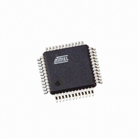
AT91SAM7S32-AU-001 Atmel, AT91SAM7S32-AU-001 Datasheet - Page 223

AT91SAM7S32-AU-001
Manufacturer Part Number
AT91SAM7S32-AU-001
Description
IC ARM7 MCU 32BIT 32K 48LQFP
Manufacturer
Atmel
Series
AT91SAMr
Specifications of AT91SAM7S32-AU-001
Core Processor
ARM7
Core Size
16/32-Bit
Speed
55MHz
Connectivity
I²C, SPI, SSC, UART/USART
Peripherals
Brown-out Detect/Reset, POR, PWM, WDT
Number Of I /o
21
Program Memory Size
32KB (32K x 8)
Program Memory Type
FLASH
Ram Size
8K x 8
Voltage - Supply (vcc/vdd)
1.65 V ~ 1.95 V
Data Converters
A/D 8x10b
Oscillator Type
Internal
Operating Temperature
-40°C ~ 85°C
Package / Case
48-LQFP
For Use With
AT91SAM7S-EK - KIT EVAL FOR ARM AT91SAM7S
Lead Free Status / RoHS Status
Lead free / RoHS Compliant
Eeprom Size
-
Other names
AT91SAM7S32-AU001
Available stocks
Company
Part Number
Manufacturer
Quantity
Price
- Current page: 223 of 779
- Download datasheet (11Mb)
26.4.7
26.4.8
6175K–ATARM–30-Aug-10
Chip Identifier
ICE Access Prevention
The Debug Communication Channel contains two registers that are accessible through the ICE
Breaker on the JTAG side and through the coprocessor 0 on the ARM Processor side.
As a reminder, the following instructions are used to read and write the Debug Communication
Channel:
Returns the debug communication data read register into Rd
Writes the value in Rd to the debug communication data write register.
The bits COMMRX and COMMTX, which indicate, respectively, that the read register has been
written by the debugger but not yet read by the processor, and that the write register has been
written by the processor and not yet read by the debugger, are wired on the two highest bits of
the status register DBGU_SR. These bits can generate an interrupt. This feature permits han-
dling under interrupt a debug link between a debug monitor running on the target system and a
debugger.
The Debug Unit features two chip identifier registers, DBGU_CIDR (Chip ID Register) and
DBGU_EXID (Extension ID). Both registers contain a hard-wired value that is read-only. The first
register contains the following fields:
The second register is device-dependent and reads 0 if the bit EXT is 0.
The Debug Unit allows blockage of access to the system through the ARM processor's ICE
interface. This feature is implemented via the register Force NTRST (DBGU_FNR), that allows
assertion of the NTRST signal of the ICE Interface. Writing the bit FNTRST (Force NTRST) to 1
in this register prevents any activity on the TAP controller.
On standard devices, the FNTRST bit resets to 0 and thus does not prevent ICE access.
This feature is especially useful on custom ROM devices for customers who do not want their
on-chip code to be visible.
• EXT - shows the use of the extension identifier register
• NVPTYP and NVPSIZ - identifies the type of embedded non-volatile memory and its size
• ARCH - identifies the set of embedded peripheral
• SRAMSIZ - indicates the size of the embedded SRAM
• EPROC - indicates the embedded ARM processor
• VERSION - gives the revision of the silicon
MRC
MCR
p14, 0, Rd, c1, c0, 0
p14, 0, Rd, c1, c0, 0
AT91SAM7S Series Preliminary
223
Related parts for AT91SAM7S32-AU-001
Image
Part Number
Description
Manufacturer
Datasheet
Request
R

Part Number:
Description:
Manufacturer:
ATMEL Corporation
Datasheet:

Part Number:
Description:
AT91 ARM Thumb-based Microcontrollers
Manufacturer:
ATMEL [ATMEL Corporation]
Datasheet:

Part Number:
Description:
IC ARM7 MCU FLASH 32K 48QFN
Manufacturer:
Atmel
Datasheet:

Part Number:
Description:
IC MCU ARM7 32KB FLASH 48LQFP
Manufacturer:
Atmel
Datasheet:

Part Number:
Description:
IC MCU ARM7 32KB FLASH 48-VQFN
Manufacturer:
Atmel
Datasheet:

Part Number:
Description:
DEV KIT FOR AVR/AVR32
Manufacturer:
Atmel
Datasheet:

Part Number:
Description:
INTERVAL AND WIPE/WASH WIPER CONTROL IC WITH DELAY
Manufacturer:
ATMEL Corporation
Datasheet:

Part Number:
Description:
Low-Voltage Voice-Switched IC for Hands-Free Operation
Manufacturer:
ATMEL Corporation
Datasheet:

Part Number:
Description:
MONOLITHIC INTEGRATED FEATUREPHONE CIRCUIT
Manufacturer:
ATMEL Corporation
Datasheet:

Part Number:
Description:
AM-FM Receiver IC U4255BM-M
Manufacturer:
ATMEL Corporation
Datasheet:

Part Number:
Description:
Monolithic Integrated Feature Phone Circuit
Manufacturer:
ATMEL Corporation
Datasheet:

Part Number:
Description:
Multistandard Video-IF and Quasi Parallel Sound Processing
Manufacturer:
ATMEL Corporation
Datasheet:


