AT91SAM7S32-AU-001 Atmel, AT91SAM7S32-AU-001 Datasheet - Page 754
AT91SAM7S32-AU-001
Manufacturer Part Number
AT91SAM7S32-AU-001
Description
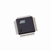
IC ARM7 MCU 32BIT 32K 48LQFP
Manufacturer
Atmel
Series
AT91SAMr
Specifications of AT91SAM7S32-AU-001
Core Processor
ARM7
Core Size
16/32-Bit
Speed
55MHz
Connectivity
I²C, SPI, SSC, UART/USART
Peripherals
Brown-out Detect/Reset, POR, PWM, WDT
Number Of I /o
21
Program Memory Size
32KB (32K x 8)
Program Memory Type
FLASH
Ram Size
8K x 8
Voltage - Supply (vcc/vdd)
1.65 V ~ 1.95 V
Data Converters
A/D 8x10b
Oscillator Type
Internal
Operating Temperature
-40°C ~ 85°C
Package / Case
48-LQFP
For Use With
AT91SAM7S-EK - KIT EVAL FOR ARM AT91SAM7S
Lead Free Status / RoHS Status
Lead free / RoHS Compliant
Eeprom Size
-
Other names
AT91SAM7S32-AU001
Available stocks
Company
Part Number
Manufacturer
Quantity
Price


40.23.4
40.23.4.1
40.23.5
40.23.5.1
40.23.5.2
40.23.5.3
754
AT91SAM7S Series Preliminary
Serial Peripheral Interface (SPI)
Synchronous Serial Controller (SSC)
SPI: Bad Serial Clock Generation on 2nd Chip Select
SSC: Periodic Transmission Limitations in Master Mode
SSC: Transmitter Limitations in Slave Mode
SSC: Transmitter Limitations in Slave Mode
Bad Serial clock generation on the 2nd chip select when SCBR = 1, CPOL = 1 and NCPHA = 0.
This occurs using SPI with the following conditions:
Do not use a multiple Chip Select configuration where at least one SCRx register is configured
with SCBR = 1 and the others differ from 1 if NCPHA = 0 and CPOL = 1.
If all chip selects are configured with Baudrate = 1, the issue does not appear.
If the Least Significant Bit is sent first (MSBF = 0), the first TAG during the frame synchro is not
sent.
None.
If TK is programmed as output and TF is programmed as input, it is impossible to emit data
when the start of edge (rising or falling) of synchro has a Start Delay equal to zero.
None.
If TK is programmed as an input and TF is programmed as an output and requested to be set to
low/high during data emission, the Frame Synchro signal is generated one bit clock period after
the data start and one data bit is lost. This problem does not exist when generating a periodic
synchro.
The data need to be delayed for one bit clock period with an external assembly.
In the following schematic, TD, TK and NRST are AT91SAM7S signals, TXD is the delayed data
to connect to the device.
• Master Mode
• CPOL = 1 and NCPHA = 0
• Multiple chip selects are used with one transfer with Baud rate (SCBR) equal to 1 (i.e., when
• Transmitting with the slowest chip select and then with the fastest one, then an additional
serial clock frequency equals the system clock frequency) and the other transfers set with
SCBR are not equal to 1
pulse is generated on output SPCK during the second transfer.
Problem Fix/Workaround
Problem Fix/Workaround
Problem Fix/Workaround
Problem Fix/Workaround
6175K–ATARM–30-Aug-10
Related parts for AT91SAM7S32-AU-001
Image
Part Number
Description
Manufacturer
Datasheet
Request
R

Part Number:
Description:
Manufacturer:
ATMEL Corporation
Datasheet:

Part Number:
Description:
AT91 ARM Thumb-based Microcontrollers
Manufacturer:
ATMEL [ATMEL Corporation]
Datasheet:

Part Number:
Description:
IC ARM7 MCU FLASH 32K 48QFN
Manufacturer:
Atmel
Datasheet:

Part Number:
Description:
IC MCU ARM7 32KB FLASH 48LQFP
Manufacturer:
Atmel
Datasheet:
Part Number:
Description:
IC MCU ARM7 32KB FLASH 48-VQFN
Manufacturer:
Atmel
Datasheet:

Part Number:
Description:
DEV KIT FOR AVR/AVR32
Manufacturer:
Atmel
Datasheet:
Part Number:
Description:
INTERVAL AND WIPE/WASH WIPER CONTROL IC WITH DELAY
Manufacturer:
ATMEL Corporation
Datasheet:
Part Number:
Description:
Low-Voltage Voice-Switched IC for Hands-Free Operation
Manufacturer:
ATMEL Corporation
Datasheet:
Part Number:
Description:
MONOLITHIC INTEGRATED FEATUREPHONE CIRCUIT
Manufacturer:
ATMEL Corporation
Datasheet:
Part Number:
Description:
AM-FM Receiver IC U4255BM-M
Manufacturer:
ATMEL Corporation
Datasheet:
Part Number:
Description:
Monolithic Integrated Feature Phone Circuit
Manufacturer:
ATMEL Corporation
Datasheet:
Part Number:
Description:
Multistandard Video-IF and Quasi Parallel Sound Processing
Manufacturer:
ATMEL Corporation
Datasheet: