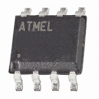
ATTINY15L-1SU Atmel, ATTINY15L-1SU Datasheet - Page 20

ATTINY15L-1SU
Manufacturer Part Number
ATTINY15L-1SU
Description
IC MCU AVR 1K FLASH 1.6MHZ 8SOIC
Manufacturer
Atmel
Series
AVR® ATtinyr
Specifications of ATTINY15L-1SU
Core Processor
AVR
Core Size
8-Bit
Speed
1.6MHz
Peripherals
Brown-out Detect/Reset, POR, PWM, WDT
Number Of I /o
6
Program Memory Size
1KB (512 x 16)
Program Memory Type
FLASH
Eeprom Size
64 x 8
Voltage - Supply (vcc/vdd)
2.7 V ~ 5.5 V
Data Converters
A/D 4x10b
Oscillator Type
Internal
Operating Temperature
-40°C ~ 85°C
Package / Case
8-SOIC (5.3mm Width), 8-SOP, 8-SOEIAJ
Lead Free Status / RoHS Status
Lead free / RoHS Compliant
Ram Size
-
Connectivity
-
Available stocks
Company
Part Number
Manufacturer
Quantity
Price
Part Number:
ATTINY15L-1SU
Manufacturer:
ATMEL/爱特梅尔
Quantity:
20 000
The General Interrupt Flag
Register – GIFR
The Timer/Counter Interrupt
Mask Register – TIMSK
20
ATtiny15L
The corresponding interrupt of External Interrupt Request 0 is executed from Program
memory address $001. See also “External Interrupts.”
• Bit 5 – PCIE: Pin Change Interrupt Enable
When the PCIE bit is set (one) and the I-bit in the Status Register (SREG) is set (one),
the interrupt on pin change is enabled. Any change on any input or I/O pin will cause an
interrupt. The corresponding interrupt of Pin Change Interrupt Request is executed from
Program memory address $002. See also “Pin Change Interrupt.”
• Bits 4..0 – Res: Reserved Bits
These bits are reserved bits in the ATtiny15L and always read as zero.
• Bit 7 – Res: Reserved Bit
This bit is a reserved bit in the ATtiny15L and always reads as zero.
• Bit 6 – INTF0: External Interrupt Flag0
When an edge or logic change on the INT0 pin triggers an interrupt request, INTF0
becomes set (one). If the I-bit in SREG and the INT0 bit in GIMSK are set (one), the
MCU will jump to the Interrupt Vector at address $001. The flag is cleared when the
interrupt routine is executed. Alternatively, the flag can be cleared by writing a logical “1”
to it. The flag is always cleared when INT0 is configured as level interrupt.
• Bit 5 – PCIF: Pin Change Interrupt Flag
When an event on any input or I/O pin triggers an interrupt request, PCIF becomes set
(one). If the I-bit in SREG and the PCIE bit in GIMSK are set (one), the MCU will jump to
the Interrupt Vector at address $002. The flag is cleared when the interrupt routine is
executed. Alternatively, the flag can be cleared by writing a logical “1” to it.
• Bits 4..0 – Res: Reserved Bits
These bits are reserved bits in the ATtiny15L and always read as zero.
• Bit 7 – Res: Reserved Bit
This bit is a reserved bit in the ATtiny15L and always reads as zero.
• Bit 6 – OCIE1A: Timer/Counter1 Output Compare Interrupt Enable
When the OCIE1A bit is set (one) and the I-bit in the Status Register is set (one), the
Timer/Counter1 Compare Match, interrupt is enabled. The corresponding interrupt (at
Bit
$3A
Read/Write
Initial Value
Bit
$39
Read/Write
Initial Value
R
7
–
0
R
7
–
0
OCIE1A
INTF0
R/W
R/W
6
0
6
0
PCIF
R/W
5
0
R
5
–
0
R
R
4
–
0
4
–
0
R
3
–
0
R
3
–
0
TOIE1
R
2
–
0
R/W
2
0
TOIE0
R
R/W
1
–
0
1
0
1187H–AVR–09/07
R
0
–
0
0
–
R
0
TIMSK
GIFR


