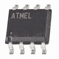
ATTINY15L-1SU Atmel, ATTINY15L-1SU Datasheet - Page 29

ATTINY15L-1SU
Manufacturer Part Number
ATTINY15L-1SU
Description
IC MCU AVR 1K FLASH 1.6MHZ 8SOIC
Manufacturer
Atmel
Series
AVR® ATtinyr
Specifications of ATTINY15L-1SU
Core Processor
AVR
Core Size
8-Bit
Speed
1.6MHz
Peripherals
Brown-out Detect/Reset, POR, PWM, WDT
Number Of I /o
6
Program Memory Size
1KB (512 x 16)
Program Memory Type
FLASH
Eeprom Size
64 x 8
Voltage - Supply (vcc/vdd)
2.7 V ~ 5.5 V
Data Converters
A/D 4x10b
Oscillator Type
Internal
Operating Temperature
-40°C ~ 85°C
Package / Case
8-SOIC (5.3mm Width), 8-SOP, 8-SOEIAJ
Lead Free Status / RoHS Status
Lead free / RoHS Compliant
Ram Size
-
Connectivity
-
Available stocks
Company
Part Number
Manufacturer
Quantity
Price
Part Number:
ATTINY15L-1SU
Manufacturer:
ATMEL/爱特梅尔
Quantity:
20 000
The Timer/Counter1 Control
Register – TCCR1
1187H–AVR–09/07
The Timer/Counter1 contains two Output Compare Registers, OCR1A and OCR1B, as
the data source to be compared with the Timer/Counter1 contents. In Normal mode the
Output Compare function is operational with OCR1A only, and the Output Compare
function includes optional clearing of the counter on compare match, and action on the
Output Compare pin (PB1) (OC1A).
In PWM mode OCR1A provides the data value against which the Timer/Counter value is
compared. Upon compare match the PWM output is generated. In PWM mode The
Timer/Counter counts up to the value specified in Output Compare Register OCR1B
and starts again from $00. This feature allows limiting the counter “full” value to a speci-
fied value, lower than $FF. However, if OCR1n is $00, the output will remain constant
and not toggle at all. If OCR1n equals $01, the pulse width will be two ticks, increasing
linearly if OCR1n is larger than $01. Together with the many prescaler options, flexible
PWM frequency selection is provided. Table 14 lists clock selection and OCR1B values
to obtain PWM frequencies from 10 kHz to 150 kHz at 10 kHz steps.
In applications with variable PWM, halving the prescaler setting and doubling the duty
cycle can be used to fine-tune the PWM. Alternatively inverted PWM can be used.
• Bit 7 – CTC1: Clear Timer/Counter on Compare Match
When the CTC1 control bit is set (one), Timer/Counter1 is reset to $00 in the CPU clock
cycle after a compare match with OCR1A Register value. If the control bit is cleared,
Timer/Counter1 continues counting and is unaffected by a compare match.
• Bit 6 – PWM1: Pulse Width Modulator Enable
When set (one), this bit enables PWM mode for Timer/Counter1. This mode is described
on page 31.
• Bits 5,4 – COM1A1, COM1A0: Compare Output Mode, Bits 1 and 0
The COM1A1 and COM1A0 control bits determine any output pin action following a
compare match A in Timer/Counter1. Output pin actions affect pin PB1(OC1A). Since
this is an alternative function to an I/O port, the corresponding direction control bit must
be set (one) to control an output pin. The control configuration is shown in Table 10.
Table 10. Compare Mode Select
Note:
Bit
$30
Read/Write
Initial Value
COM1A1
0
0
1
1
1. In PWM mode, these bits have a different function. Refer to Table 12 for a detailed
description.When changing the COM1A1/COM1A0 bits, the Output Compare 1A
Interrupt must be disabled by clearing its Interrupt Enable bit in the TIMSK Register.
Otherwise an interrupt can occur when the bits are changed.
CTC1
R/W
7
0
COM1A0
0
1
0
1
PWM1
R/W
6
0
Description
Timer/Counter disconnected from output pin OC1A
Toggle the OC1A output line.
Clear the OC1A output line (to zero).
Set the OC1A output line (to one).
COM1A1
R/W
5
0
(1)
COM1A0
R/W
4
0
CS13
R/W
3
0
CS12
R/W
2
0
CS11
R/W
1
0
ATtiny15L
CS10
R/W
0
0
TCCR1
29


