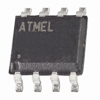
ATTINY15L-1SU Atmel, ATTINY15L-1SU Datasheet - Page 31

ATTINY15L-1SU
Manufacturer Part Number
ATTINY15L-1SU
Description
IC MCU AVR 1K FLASH 1.6MHZ 8SOIC
Manufacturer
Atmel
Series
AVR® ATtinyr
Specifications of ATTINY15L-1SU
Core Processor
AVR
Core Size
8-Bit
Speed
1.6MHz
Peripherals
Brown-out Detect/Reset, POR, PWM, WDT
Number Of I /o
6
Program Memory Size
1KB (512 x 16)
Program Memory Type
FLASH
Eeprom Size
64 x 8
Voltage - Supply (vcc/vdd)
2.7 V ~ 5.5 V
Data Converters
A/D 4x10b
Oscillator Type
Internal
Operating Temperature
-40°C ~ 85°C
Package / Case
8-SOIC (5.3mm Width), 8-SOP, 8-SOEIAJ
Lead Free Status / RoHS Status
Lead free / RoHS Compliant
Ram Size
-
Connectivity
-
Available stocks
Company
Part Number
Manufacturer
Quantity
Price
Part Number:
ATTINY15L-1SU
Manufacturer:
ATMEL/爱特梅尔
Quantity:
20 000
Timer/Counter1 Output
Compare RegisterA – OCR1A
Timer/Counter1 in PWM Mode
1187H–AVR–09/07
The Output Compare Register 1A is an 8-bit read/write register.
The Timer/Counter Output Compare Register 1A contains the data to be continuously
compared with Timer/Counter1. Actions on compare matches are specified in TCCR1. A
compare match occurs only if Timer/Counter1 counts to the OCR1A value. A software
write that sets TCNT1 and OCR1A to the same value does not generate a compare
match.
A compare match will set (one) the Compare Interrupt Flag in the CPU clock cycle fol-
lowing the compare event.
When the PWM mode is selected, Timer/Counter1 and the Output Compare Register A
(OCR1A) form an 8-bit, free-running and glitch-free PWM with outputs on the
PB1(OC1A) pin. Timer/Counter1 acts as an up-counter, counting up from $00 up to the
value specified in the second Output Compare Register OCR1B, and starting from $00
up again. When the counter value matches the contents of the Output Compare Regis-
ter OCR1A, the PB1(OC1A) pin is set or cleared according to the settings of the
COM1A1/COM1A0 bits in the Timer/Counter1 Control Registers TCCR1. Refer to Table
12 for details.
Table 12. Compare Mode Select in PWM Mode
Note that in PWM mode, writing to the Output Compare OCR1A, the data value is first
transferred to a temporary location. The value is latched into OCR1A when the
Timer/Counter reaches OCR1B. This prevents the occurrence of odd-length PWM
pulses (glitches) in the event of an unsynchronized OCR1A write. See Figure 22 for an
example.
Bit
$2E
Read/Write
Initial Value
COM1A1
0
0
1
1
COM1A0
MSB
R/W
7
0
0
1
0
1
R/W
6
0
Effect on Compare Pin
Not connected
Not connected
Cleared on compare match (up-counting) (non-inverted PWM). Set
when TCNT1 = $00.
Set on compare match (up-counting) (inverted PWM). Cleared when
TCNT1 = $00.
R/W
5
0
R/W
4
0
R/W
3
0
R/W
2
0
R/W
1
0
ATtiny15L
LSB
R/W
0
0
OCR1A
31


