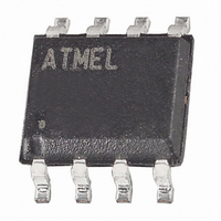
ATTINY15L-1SU Atmel, ATTINY15L-1SU Datasheet - Page 41

ATTINY15L-1SU
Manufacturer Part Number
ATTINY15L-1SU
Description
IC MCU AVR 1K FLASH 1.6MHZ 8SOIC
Manufacturer
Atmel
Series
AVR® ATtinyr
Specifications of ATTINY15L-1SU
Core Processor
AVR
Core Size
8-Bit
Speed
1.6MHz
Peripherals
Brown-out Detect/Reset, POR, PWM, WDT
Number Of I /o
6
Program Memory Size
1KB (512 x 16)
Program Memory Type
FLASH
Eeprom Size
64 x 8
Voltage - Supply (vcc/vdd)
2.7 V ~ 5.5 V
Data Converters
A/D 4x10b
Oscillator Type
Internal
Operating Temperature
-40°C ~ 85°C
Package / Case
8-SOIC (5.3mm Width), 8-SOP, 8-SOEIAJ
Lead Free Status / RoHS Status
Lead free / RoHS Compliant
Ram Size
-
Connectivity
-
Available stocks
Company
Part Number
Manufacturer
Quantity
Price
Part Number:
ATTINY15L-1SU
Manufacturer:
ATMEL/爱特梅尔
Quantity:
20 000
The Analog-to-Digital
Converter, Analog
Multiplexer, and Gain
Stages
Features
1187H–AVR–09/07
•
•
•
•
•
•
•
•
•
•
•
•
•
•
•
The ATtiny15L features a 10-bit successive approximation ADC. The ADC is connected
to a 4-channel Analog Multiplexer that allows one differential voltage input and four sin-
gle-ended voltage inputs constructed from the pins of Port B. The differential input (PB3,
PB4) is equipped with a programmable gain stage, providing amplification step of 26 dB
(20x) on the differential input voltage before the A/D conversion. The single-ended volt-
age inputs at PB2..PB5 refer to 0V (GND).
The ADC contains a Sample and Hold Amplifier that ensures that the input voltage to
the ADC is held at a constant level during conversion. A block diagram of the ADC is
shown in Figure 25.
An internal reference voltage of nominally 2.56V is provided On-chip and this reference
can optionally be externally decoupled at the AREF (PB0) pin by a capacitor for better
noise performance. Alternatively, V
ended channels. There is also an option to use an external voltage reference and turn
off the internal voltage reference. These options are selected using the REFS1..0 bits of
the ADMUX Control Register.
10-bit Resolution
±2 LSB Absolute Accuracy
0.5 LSB Integral Non-linearity
Optional Offset Cancellation
65 - 260 µs Conversion Time
Up to 15 kSPS
4 Multiplexed Single-ended Input Channels
1 Differential Input Channel with Optional Gain of 20x
2.56V Internal Voltage Reference
0 - 2.56V Differential Input Voltage Range
0 - V
Optional Left Adjustment for ADC Result Readout
Free Running or Single Conversion Mode
Interrupt on ADC Conversion Complete
Sleep Mode Noise Canceler
CC
Single-ended Input Voltage Range
CC
can be used as reference voltage for single-
ATtiny15L
41


