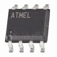
ATTINY15L-1SU Atmel, ATTINY15L-1SU Datasheet - Page 24

ATTINY15L-1SU
Manufacturer Part Number
ATTINY15L-1SU
Description
IC MCU AVR 1K FLASH 1.6MHZ 8SOIC
Manufacturer
Atmel
Series
AVR® ATtinyr
Specifications of ATTINY15L-1SU
Core Processor
AVR
Core Size
8-Bit
Speed
1.6MHz
Peripherals
Brown-out Detect/Reset, POR, PWM, WDT
Number Of I /o
6
Program Memory Size
1KB (512 x 16)
Program Memory Type
FLASH
Eeprom Size
64 x 8
Voltage - Supply (vcc/vdd)
2.7 V ~ 5.5 V
Data Converters
A/D 4x10b
Oscillator Type
Internal
Operating Temperature
-40°C ~ 85°C
Package / Case
8-SOIC (5.3mm Width), 8-SOP, 8-SOEIAJ
Lead Free Status / RoHS Status
Lead free / RoHS Compliant
Ram Size
-
Connectivity
-
Available stocks
Company
Part Number
Manufacturer
Quantity
Price
Part Number:
ATTINY15L-1SU
Manufacturer:
ATMEL/爱特梅尔
Quantity:
20 000
ADC Noise Reduction Mode
Power-down Mode
Tuneable Internal RC
Oscillator
The System Clock Oscillator
Calibration Register –
OSCCAL
Internal PLL for Fast
Peripheral Clock
Generation
24
ATtiny15L
When the SM1/SM0 bits are “01”, the SLEEP instruction forces the MCU into the ADC
Noise Reduction mode, stopping the CPU but allowing the ADC, the external interrupt
pin, pin change interrupt and the Watchdog (if enabled) to continue operating. Please
note that the clock system including the PLL is also active in the ADC Noise Reduction
mode. This improves the noise environment for the ADC, enabling higher resolution
measurements. If the ADC is enabled, a conversion starts automatically when this mode
is entered. In addition to Watchdog Time-out and External Reset, only an external level-
triggered interrupt, a pin change interrupt or an ADC interrupt can wake up the MCU.
When the SM1/SM0 bits are “10”, the SLEEP instruction forces the MCU into the Power-
down mode. Only an External Reset, a Watchdog Reset (if enabled), an external level-
triggered interrupt, or a pin change interrupt can wake up the MCU.
Note that if a level-triggered or pin change interrupt is used for wake-up from Power-
down mode, the changed level must be held for some time to wake up the MCU. This
makes the MCU less sensitive to noise. The changed level is sampled twice by the
Watchdog Oscillator clock, and if the input has the required level during this time, the
MCU will wake up. The period of the Watchdog Oscillator is 2.9
25°C. The frequency of the Watchdog Oscillator is voltage-dependent as shown in the
“Electrical Characteristics” section.
When waking up from the Power-down mode, a delay from the wake-up condition
occurs until the wake-up becomes effective. This allows the clock to restart and become
stable after having been stopped. The wake-up period is defined by the same CKSEL
Fuses that define the Reset Time-out period.
The internal RC Oscillator provides a fixed 1.6 MHz clock (nominal at 5V and 25°C).
This internal clock is always the system clock of the ATtiny15L. This Oscillator can be
calibrated by writing the calibration byte (see page 55) to the OSCCAL Register.
Writing the calibration byte to this address will trim the internal Oscillator frequency in
order to remove process variations. When OSCCAL is zero (initial value), the lowest
available frequency is chosen. Writing non-zero values to this register will increase the
frequency of the internal oscillator. Writing $FF to the register selects the highest avail-
able frequency.
The internal PLL in ATtiny15L generates a clock frequency that is 16x multiplied from
the RC Oscillator system clock. If the RC Oscillator frequency is the nominal 1.6 MHz,
the fast peripheral clock is 25.6 MHz. The fast peripheral clock, or a clock prescaled
from that, can be selected as the clock source for Timer/Counter1.
The PLL is locked on the tunable internal RC Oscillator and adjusting the tunable inter-
nal RC oscillator via the OSCCAL Register will adjust the fast peripheral clock at the
same time. Timer1 may malfunction if the internal RC oscillator is adjusted beyond 1.75
MHz.
It is recommended not to take the OSCCAL adjustments to a higher frequency than
1.75 MHz in order to keep proper operation of all chip functions.
Bit
$31
Read/Write
Initial Value
CAL7
R/W
7
0
CAL6
R/W
6
0
CAL5
R/W
5
0
CAL4
R/W
4
0
CAL3
R/W
3
0
CAL2
R/W
2
0
µs
CAL1
R/W
1
0
(nominal) at 3.0V and
CAL0
R/W
0
0
1187H–AVR–09/07
OSCCAL


