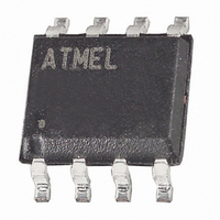
ATTINY15L-1SU Atmel, ATTINY15L-1SU Datasheet - Page 9

ATTINY15L-1SU
Manufacturer Part Number
ATTINY15L-1SU
Description
IC MCU AVR 1K FLASH 1.6MHZ 8SOIC
Manufacturer
Atmel
Series
AVR® ATtinyr
Specifications of ATTINY15L-1SU
Core Processor
AVR
Core Size
8-Bit
Speed
1.6MHz
Peripherals
Brown-out Detect/Reset, POR, PWM, WDT
Number Of I /o
6
Program Memory Size
1KB (512 x 16)
Program Memory Type
FLASH
Eeprom Size
64 x 8
Voltage - Supply (vcc/vdd)
2.7 V ~ 5.5 V
Data Converters
A/D 4x10b
Oscillator Type
Internal
Operating Temperature
-40°C ~ 85°C
Package / Case
8-SOIC (5.3mm Width), 8-SOP, 8-SOEIAJ
Lead Free Status / RoHS Status
Lead free / RoHS Compliant
Ram Size
-
Connectivity
-
Available stocks
Company
Part Number
Manufacturer
Quantity
Price
Part Number:
ATTINY15L-1SU
Manufacturer:
ATMEL/爱特梅尔
Quantity:
20 000
Subroutine and Interrupt
Hardware Stack
The EEPROM Data
Memory
Memory Access and
Instruction Execution Timing
1187H–AVR–09/07
Constant byte address is specified by the Z-register contents. The 15 MSBs select word
address (0 - 511), and LSB selects low byte if cleared (LSB = 0) or high byte if set
(LSB = 1).
The ATtiny15L uses a 3-level-deep Hardware Stack for subroutines and interrupts. The
Hardware Stack is nine bits wide and stores the Program Counter (PC) return address
while subroutines and interrupts are executed.
RCALL instructions and interrupts push the PC return address onto Stack level 0, and
the data in the other Stack levels 1 - 2 are pushed one level deeper in the Stack. When
a RET or RETI instruction is executed the returning PC is fetched from Stack level 0,
and the data in the other Stack levels 1 - 2 are popped one level in the Stack.
If more than three subsequent subroutine calls or interrupts are executed, the first val-
ues written to the Stack are overwritten. Pushing four return addresses A1, A2, A3, and
A4 followed by four subroutine or interrupt returns, will pop A4, A3, A2, and once more
A2 from the Hardware Stack.
The ATtiny15L contains 64 bytes of data EEPROM memory. It is organized as a sepa-
rate data space, in which single bytes can be read and written. The EEPROM has an
endurance of at least 100,000 write/erase cycles. The access between the EEPROM
and the CPU is described on page 36, specifying the EEPROM Address Register, the
EEPROM Data Register, and the EEPROM Control Register.
This section describes the general access timing concepts for instruction execution and
internal memory access.
The AVR CPU is driven by the System Clock Ø, directly generated from the external
clock crystal for the chip. No internal clock division is used.
Figure 10 shows the parallel instruction fetches and instruction executions enabled by
the Harvard architecture and the fast-access Register File concept. This is the basic
pipelining concept to obtain up to 1 MIPS per MHz with the corresponding unique results
for functions per cost, functions per clocks, and functions per power-unit.
Figure 10. The Parallel Instruction Fetches and Instruction Executions
Figure 11 shows the internal timing concept for the Register File. In a single clock cycle
an ALU operation using two register operands is executed, and the result is stored back
to the destination register.
2nd Instruction Execute
3rd Instruction Execute
1st Instruction Execute
2nd Instruction Fetch
3rd Instruction Fetch
4th Instruction Fetch
1st Instruction Fetch
System Clock Ø
T1
T2
T3
ATtiny15L
T4
9


