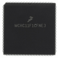
MCHC11F1CFNE3 Freescale Semiconductor, MCHC11F1CFNE3 Datasheet - Page 51

MCHC11F1CFNE3
Manufacturer Part Number
MCHC11F1CFNE3
Description
IC MCU 8BIT 1K RAM 68-PLCC
Manufacturer
Freescale Semiconductor
Series
HC11r
Specifications of MCHC11F1CFNE3
Core Processor
HC11
Core Size
8-Bit
Speed
3MHz
Connectivity
SCI, SPI
Peripherals
POR, WDT
Number Of I /o
30
Program Memory Type
ROMless
Eeprom Size
512 x 8
Ram Size
1K x 8
Voltage - Supply (vcc/vdd)
4.75 V ~ 5.25 V
Data Converters
A/D 8x8b
Oscillator Type
Internal
Operating Temperature
-40°C ~ 85°C
Package / Case
68-PLCC
A/d Inputs
8-Channel, 8-Bit
Eeprom Memory
512 Bytes
Input Output
30
Interface
SCI/SPI
Memory Type
EPROM
Number Of Bits
8
Package Type
68-pin PLCC
Programmable Memory
0 Bytes
Timers
3-16-bit
Voltage, Range
3-5.5 V
Controller Family/series
68HC11
No. Of I/o's
30
Eeprom Memory Size
512Byte
Ram Memory Size
1KB
Cpu Speed
3MHz
No. Of Timers
1
Embedded Interface Type
SCI, SPI
Rohs Compliant
Yes
Processor Series
HC11F
Core
HC11
Data Bus Width
8 bit
Program Memory Size
512 B
Data Ram Size
1 KB
Interface Type
SCI, SPI
Maximum Clock Frequency
3 MHz
Number Of Timers
1
Maximum Operating Temperature
+ 85 C
Mounting Style
SMD/SMT
Minimum Operating Temperature
- 40 C
On-chip Adc
8 bit, 8 Channel
Lead Free Status / RoHS Status
Lead free / RoHS Compliant
Program Memory Size
-
Lead Free Status / Rohs Status
RoHS Compliant part
Available stocks
Company
Part Number
Manufacturer
Quantity
Price
Company:
Part Number:
MCHC11F1CFNE3
Manufacturer:
FREESCALE
Quantity:
5 530
Company:
Part Number:
MCHC11F1CFNE3
Manufacturer:
FREESCALE
Quantity:
5 530
Company:
Part Number:
MCHC11F1CFNE3
Manufacturer:
Freescale Semiconductor
Quantity:
10 000
Company:
Part Number:
MCHC11F1CFNE3R
Manufacturer:
Freescale Semiconductor
Quantity:
10 000
OPT2 — System Configuration Options 2
GWOM — Port G Wired-OR Mode
CWOM — Port C Wired-OR Mode
CLK4X — 4XOUT Clock Enable
Bits [4:0] — Not implemented
4.3.2.5 Block Protect Register (BPROT)
BPROT — Block Protect
Bits [7:5] — Not implemented
PTCON — Protect for CONFIG
BPRT[3:0] — Block Protect Bits for EEPROM
TECHNICAL DATA
RESET:
RESET:
Refer to SECTION 6 PARALLEL INPUT/OUTPUT.
Refer to SECTION 6 PARALLEL INPUT/OUTPUT.
The 4XOUT signal, when enabled, is a buffered XTAL signal and is four times the fre-
quency of the E-clock. This buffered clock is intended to synchronize external devices
with the MCU. Refer to SECTION 2 PIN DESCRIPTIONS.
Always read zero
BPROT prevents accidental writes to EEPROM and the CONFIG register. The bits in
this register can be written to zero during the first 64 E-clock cycles after reset in the
normal modes. Once the bits are cleared to zero, the EEPROM array and the CONFIG
register can be programmed or erased. Setting the bits in the BPROT register to logic
one protects the EEPROM and CONFIG register until the next reset. Refer to Table
4-6.
Always read zero
0 = Port G operates normally.
1 = Port G outputs are open-drain type.
0 = Port C operates normally.
1 = Port C outputs are open-drain type.
0 = The 4XOUT pin is driven low.
1 = The 4XOUT signal is driven on the 4XOUT pin.
0 = CONFIG register can be programmed or erased normally
1 = CONFIG register cannot be programmed or erased
0 = Protection disabled for associated block
1 = Protection enabled for associated block
GWOM
Bit 7
Bit 7
—
0
0
CWOM
—
6
0
6
0
Freescale Semiconductor, Inc.
OPERATING MODES AND ON-CHIP MEMORY
For More Information On This Product,
CLK4X
—
5
0
5
0
Go to: www.freescale.com
PTCON
—
4
0
4
1
BPRT3
—
1
3
0
3
BPRT2
—
2
0
2
1
BPRT1
—
1
0
1
1
BPRT0
Bit 0
Bit 0
—
0
1
$1038
$1035
4-13


