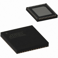
ATA5428-PLQW Atmel, ATA5428-PLQW Datasheet - Page 26

ATA5428-PLQW
Manufacturer Part Number
ATA5428-PLQW
Description
IC TXRX WIDEBND 433/868MHZ 48QFN
Manufacturer
Atmel
Specifications of ATA5428-PLQW
Frequency
433MHz, 868MHz
Data Rate - Maximum
20kbps
Modulation Or Protocol
ASK, FSK
Applications
Alarm and Security Systems, RKE
Power - Output
10dBm
Sensitivity
-112.5dBm
Voltage - Supply
2.4 V ~ 3.6 V or 4.4 V ~ 6.6 V
Current - Receiving
10.5mA
Current - Transmitting
10mA
Data Interface
PCB, Surface Mount
Antenna Connector
PCB, Surface Mount
Operating Temperature
-40°C ~ 85°C
Package / Case
48-VQFN Exposed Pad, 48-HVQFN, 48-SQFN, 48-DHVQFN
Operating Temperature (min)
-40C
Operating Temperature (max)
85C
Operating Temperature Classification
Industrial
Product Depth (mm)
7mm
Product Height (mm)
0.9mm
Product Length (mm)
7mm
Lead Free Status / RoHS Status
Lead free / RoHS Compliant
Memory Size
-
Lead Free Status / Rohs Status
Compliant
Other names
ATA5428-PLQHCT
ATA5428-PLQHCT
ATA5428-PLQWCT
ATA5428-PLQHCT
ATA5428-PLQWCT
Available stocks
Company
Part Number
Manufacturer
Quantity
Price
Company:
Part Number:
ATA5428-PLQW
Manufacturer:
LITELINK
Quantity:
106
Part Number:
ATA5428-PLQW
Manufacturer:
ATMEL/爱特梅尔
Quantity:
20 000
26
ATA5423/ATA5425/ATA5428/ATA5429
C
enter the steep region of pulling versus load capacitance where there is a risk of an unstable
oscillation.
To ensure proper start-up behavior the small signal gain, and thus the negative resistance, pro-
vided by this XTO at start is very large; for example, oscillation starts up even in worst case with
a crystal series resistance of 1.5
approximately given by
with Z
Z
Z
Z
XTAL2 with typically 19 mS at 25°C.
With f
tance of about 2 k . The worst case for technological, temperature and supply voltage variations
is then for C
Due to the large gain at startup, the XTO is able to meet a very low start-up time. The oscillation
start-up time can be estimated with the time constant
After 10
High if the amplitude is large enough. This sets N_RESET to High and activates the CLK output
if CLK_ON in control register 3 is High (see
VSOUT and DVCC voltage also have to be fulfilled (see
To save current in IDLE and Sleep modes, the load capacitors are partially switched off in these
modes with S1 and S2, as seen in
It is recommended to use a crystal with C
C
Lower values of C
higher values of C
Re Z
1
3
3
0
0
=
consists of crystals C
= –j/(2
of the XTAL has to be lower than C
= 1.0 pF to 2.2 pF.
= –j/(2
-----------------------------------------------------------------------------------------------------------
4
XTOcore
XTO
1
, Z
2
2
= 13.5 MHz, gm = 19 mS, C
to 20
as complex impedances at pin XTAL1 and XTAL2, hence
0
=
f
2
m
2.2 pF always higher than 1.5 k
Re
f
f
C
XTO
XTO
m
m
an amplitude detector detects the oscillation amplitude and sets XTO_OK to
m
Z
----------------------------------------------------------------------------------------------------- -
1
(up to 15 fF) can also be used, this has only little influence on pulling.
can be used, this increases the start-up time slightly. Lower values of C
2
Re Z
Z
C
Z
C
0
3
1
0
in parallel with an internal 110 k resistor hence
L1
+
) /110 k , gm is the internal transconductance between XTAL1 and
+
) + 5 and Z
Z
Z
XTOcore
2
2
+
Z
Z
3
3
Figure
k
+
+
+
Z
Z
R
1
at C
1
L
m
Lmin
= 9 pF, and C
2
Z
Z
= –j/(2
4-2.
0
/2 = 3.7 pF for a Pierce oscillator type in order to not
2
2
Table
2.2 pF with this XTO. The negative resistance is
m
g
Z
m
= 3.0 fF to 7.0 fF, C
3
7-7). Note that the necessary conditions of the
g
m
0
f
= 2.2 pF, this results in a negative resis-
XTO
Figure 4-2
C
L2
) + 5 .
and
LN
= 9 pF, R
Figure
5-1).
4841D–WIRE–10/07
m
< 120
and
0
or


