ATA5428-PLQW Atmel, ATA5428-PLQW Datasheet - Page 80
ATA5428-PLQW
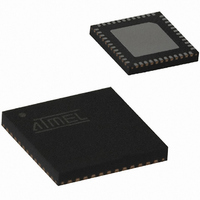
Manufacturer Part Number
ATA5428-PLQW
Description
IC TXRX WIDEBND 433/868MHZ 48QFN
Manufacturer
Atmel
Specifications of ATA5428-PLQW
Frequency
433MHz, 868MHz
Data Rate - Maximum
20kbps
Modulation Or Protocol
ASK, FSK
Applications
Alarm and Security Systems, RKE
Power - Output
10dBm
Sensitivity
-112.5dBm
Voltage - Supply
2.4 V ~ 3.6 V or 4.4 V ~ 6.6 V
Current - Receiving
10.5mA
Current - Transmitting
10mA
Data Interface
PCB, Surface Mount
Antenna Connector
PCB, Surface Mount
Operating Temperature
-40°C ~ 85°C
Package / Case
48-VQFN Exposed Pad, 48-HVQFN, 48-SQFN, 48-DHVQFN
Operating Temperature (min)
-40C
Operating Temperature (max)
85C
Operating Temperature Classification
Industrial
Product Depth (mm)
7mm
Product Height (mm)
0.9mm
Product Length (mm)
7mm
Lead Free Status / RoHS Status
Lead free / RoHS Compliant
Memory Size
-
Lead Free Status / Rohs Status
Compliant
Other names
ATA5428-PLQHCT
ATA5428-PLQHCT
ATA5428-PLQWCT
ATA5428-PLQHCT
ATA5428-PLQWCT
Available stocks
Company
Part Number
Manufacturer
Quantity
Price
Company:

Part Number:
ATA5428-PLQW
Manufacturer:
LITELINK
Quantity:
106
Part Number:
ATA5428-PLQW
Manufacturer:
ATMEL/爱特梅尔
Quantity:
20 000


12. Electrical Characteristics: General (Continued)
This device is manufactured with an industrial (not automotive) grade process and process controls. Although this device may
meet certain automotive grade criteria in performance, Atmel can not recommend that this device be used in any automotive
application.
All parameters refer to GND and are valid for T
and V
about current consumption, timing and digital pin properties can be found in the specific sections of the “Electrical Characteristics”.
80
*) Type means: A = 100% tested, B = 100% correlation tested, C = Characterized on samples, D = Design parameter
Note:
No. Parameters
5.1 Spurious TX mode
5.2 Spurious RX mode
5.3
5.4
5.5
5
VS2
Synthesizer
In loop phase noise
TX mode
Phase noise at 1M
RX mode
Phase noise at 1M
TX mode
= V
1. Pin numbers in brackets mean they were measured with RF_IN matched to 50 according to
ATA5423/ATA5425/ATA5428/ATA5429
VAUX
component values according to
with component values according to
= 5.0V (Base
-
station Application). Typical values are given at f
Test Conditions
At ±f
f
f
f
f
f
At ±f
f
f
f
f
f
At ±f
f
f
f
f
f
At ±f
f
f
f
f
f
Measured at 20 kHz
distance to carrier
f
f
f
f
f
f
f
f
f
f
f
f
f
f
f
RF
RF
RF
RF
RF
RF
RF
RF
RF
RF
RF
RF
RF
RF
RF
RF
RF
RF
RF
RF
RF
RF
RF
RF
RF
RF
RF
RF
RF
RF
RF
RF
RF
RF
RF
= 315 MHz
= 345 MHz
= 433.92 MHz
= 868.3 MHz
= 915 MHz
= 315 MHz
= 345 MHz
= 433.92 MHz
= 868.3 MHz
= 915 MHz
= 315 MHz
= 345 MHz
= 433.92 MHz
= 868.3 MHz
= 915 MHz
= 315 MHz
= 345 MHz
= 433.92 MHz
= 868.3 MHz
= 915 MHz
= 315 MHz
= 345 MHz
= 433.92 MHz
= 868.3 MHz
= 915 MHz
= 315 MHz
= 345 MHz
= 433.92 MHz
= 868.3 MHz
= 915 MHz
= 315 MHz
= 345 MHz
= 433.92 MHz
= 868.3 MHz
= 915 MHz
CLK
XTO
CLK
XTO
, CLK enabled
, CLK enabled
Table 3-2 on page 12
amb
Table 3-7 on page
= 25°C, V
VS1
Pin
= V
(1)
VS2
and RF_OUT matched to 50 according to
22.
= 3.0V (1
Symbol
L
L
SP
SP
L
SP
SP
TX20k
RX1M
TX1M
TX
TX
RX
RX
-
RF
battery application), V
= 433.92 MHz unless otherwise specified. Details
Min.
<
<
<
<
<
–
–
–
–
–
–
–
–
–
–
Typ.
–
–
–
–
–
–
–
–
–
–
–
–
–
–
–
–
–
–
–
–
121
120
120
113
113
113
113
111
107
107
–
–
–
–
–
72
74
68
70
69
70
68
66
60
60
75
73
75
68
67
85
85
80
75
75
75
75
75
75
75
VS2
= 6.0V (2-battery application)
Figure 3-1 on page 11
Figure 3-10 on page 21
Max.
dBC/Hz
dBC/Hz
dBC/Hz
4841D–WIRE–10/07
Unit
dBC
dBC
dBC
dBC
Type*
with
C
C
C
C
A
C
C
Related parts for ATA5428-PLQW
Image
Part Number
Description
Manufacturer
Datasheet
Request
R

Part Number:
Description:
RF Transceiver ASK/FSK Transceiver 434 and 868MHz
Manufacturer:
Atmel
Datasheet:
Part Number:
Description:
RF Transceiver ASK/FSK Transceiver 434 and 868MHz
Manufacturer:
Atmel
Datasheet:
Part Number:
Description:
RF Transceiver ASK/FSK Transceiver 434 and 868 MHz
Manufacturer:
Atmel
Datasheet:

Part Number:
Description:
Manufacturer:
Atmel
Datasheet:
Part Number:
Description:
Manufacturer:
Atmel
Datasheet:

Part Number:
Description:
Uhf Ask/fsk Transceiver
Manufacturer:
ATMEL Corporation
Datasheet:

Part Number:
Description:
DEV KIT FOR AVR/AVR32
Manufacturer:
Atmel
Datasheet:
Part Number:
Description:
INTERVAL AND WIPE/WASH WIPER CONTROL IC WITH DELAY
Manufacturer:
ATMEL Corporation
Datasheet:
Part Number:
Description:
Low-Voltage Voice-Switched IC for Hands-Free Operation
Manufacturer:
ATMEL Corporation
Datasheet:
Part Number:
Description:
MONOLITHIC INTEGRATED FEATUREPHONE CIRCUIT
Manufacturer:
ATMEL Corporation
Datasheet:
Part Number:
Description:
AM-FM Receiver IC U4255BM-M
Manufacturer:
ATMEL Corporation
Datasheet:
Part Number:
Description:
Monolithic Integrated Feature Phone Circuit
Manufacturer:
ATMEL Corporation
Datasheet: