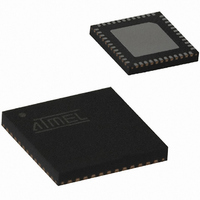
ATA5428-PLQW Atmel, ATA5428-PLQW Datasheet - Page 46

ATA5428-PLQW
Manufacturer Part Number
ATA5428-PLQW
Description
IC TXRX WIDEBND 433/868MHZ 48QFN
Manufacturer
Atmel
Specifications of ATA5428-PLQW
Frequency
433MHz, 868MHz
Data Rate - Maximum
20kbps
Modulation Or Protocol
ASK, FSK
Applications
Alarm and Security Systems, RKE
Power - Output
10dBm
Sensitivity
-112.5dBm
Voltage - Supply
2.4 V ~ 3.6 V or 4.4 V ~ 6.6 V
Current - Receiving
10.5mA
Current - Transmitting
10mA
Data Interface
PCB, Surface Mount
Antenna Connector
PCB, Surface Mount
Operating Temperature
-40°C ~ 85°C
Package / Case
48-VQFN Exposed Pad, 48-HVQFN, 48-SQFN, 48-DHVQFN
Operating Temperature (min)
-40C
Operating Temperature (max)
85C
Operating Temperature Classification
Industrial
Product Depth (mm)
7mm
Product Height (mm)
0.9mm
Product Length (mm)
7mm
Lead Free Status / RoHS Status
Lead free / RoHS Compliant
Memory Size
-
Lead Free Status / Rohs Status
Compliant
Other names
ATA5428-PLQHCT
ATA5428-PLQHCT
ATA5428-PLQWCT
ATA5428-PLQHCT
ATA5428-PLQWCT
Available stocks
Company
Part Number
Manufacturer
Quantity
Price
Company:
Part Number:
ATA5428-PLQW
Manufacturer:
LITELINK
Quantity:
106
Part Number:
ATA5428-PLQW
Manufacturer:
ATMEL/爱特梅尔
Quantity:
20 000
7.6
Figure 7-4.
46
Pin PWR_ON
ATA5423/ATA5425/ATA5428/ATA5429
(Status register)
DVCC, AVCC
Timing Pin PWR_ON, Status Bit Power_On
Power_ON
N_RESET
PWR_ON
VSOUT
CLK
IRQ
To switch the transceiver from OFF to IDLE mode, pin PWR_ON must be set to “1” (minimum
0.8
sets pin N_RESET to low, and switches on DVCC, AVCC and the power supply for external
devices VSOUT.
If V
sets the status bit Power_On to “1” and an interrupt is issued (T
After the voltage on pin VSOUT exceeds 2.3V (typically) and the start-up time of the XTO is
elapsed the output clock on pin CLK is available. Because the enabling of pin CLK is asynchro-
nous, the first clock cycle may be incomplete. N_RESET is set to high if V
(typically) and the XTO is settled.
If the transceiver is in any active mode (IDLE, AUX, RX, RX_Polling, TX), a positive edge on pin
PWR_ON sets Power_On to “1” (after T
erates an interrupt. If Power_On is still “1” during the positive edge on pin PWR_ON no interrupt
is issued. Power_On and the interrupt are deleted after reading the status register.
During Power_On = 1, the bits VSOUT_EN and CLK_ON in control register 3 are set to “1”.
Note:
1.5V (typ)
Mode
OFF
V
DVCC
Thres_2
V
VS2
It is not possible to set the transceiver to OFF mode by setting pin PWR_ON to “0”. If pin
PWR_ON is not used, it must be connected to GND.
exceeds 1.5V (typically) and the XTO is settled, the digital control logic is active and
= 2.38V (typ)
) for at least T
T
T
PWR_ON
PWR_ON_IRQ_1
Mode
IDLE
> T
PWR_ON_IRQ_1
V
Thres_1
PWR_ON
(typ)
= 2.V
(see
Figure
PWR_ON_IRQ_2
T
PWR_ON
IDLE, AUX, RX, RX Polling, TX
7-4). The transceiver recognizes the positive edge,
> T
T
PWR_ON_IRQ_2
PWR_ON_IRQ_2
). The state transition Power_On 0
Mode
PWR_ON_IRQ_1
VSOUT
).
exceeds 2.38V
4841D–WIRE–10/07
1 gen-


