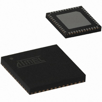
ATA5428-PLQW Atmel, ATA5428-PLQW Datasheet - Page 44

ATA5428-PLQW
Manufacturer Part Number
ATA5428-PLQW
Description
IC TXRX WIDEBND 433/868MHZ 48QFN
Manufacturer
Atmel
Specifications of ATA5428-PLQW
Frequency
433MHz, 868MHz
Data Rate - Maximum
20kbps
Modulation Or Protocol
ASK, FSK
Applications
Alarm and Security Systems, RKE
Power - Output
10dBm
Sensitivity
-112.5dBm
Voltage - Supply
2.4 V ~ 3.6 V or 4.4 V ~ 6.6 V
Current - Receiving
10.5mA
Current - Transmitting
10mA
Data Interface
PCB, Surface Mount
Antenna Connector
PCB, Surface Mount
Operating Temperature
-40°C ~ 85°C
Package / Case
48-VQFN Exposed Pad, 48-HVQFN, 48-SQFN, 48-DHVQFN
Operating Temperature (min)
-40C
Operating Temperature (max)
85C
Operating Temperature Classification
Industrial
Product Depth (mm)
7mm
Product Height (mm)
0.9mm
Product Length (mm)
7mm
Lead Free Status / RoHS Status
Lead free / RoHS Compliant
Memory Size
-
Lead Free Status / Rohs Status
Compliant
Other names
ATA5428-PLQHCT
ATA5428-PLQHCT
ATA5428-PLQWCT
ATA5428-PLQHCT
ATA5428-PLQWCT
Available stocks
Company
Part Number
Manufacturer
Quantity
Price
Company:
Part Number:
ATA5428-PLQW
Manufacturer:
LITELINK
Quantity:
106
Part Number:
ATA5428-PLQW
Manufacturer:
ATMEL/爱特梅尔
Quantity:
20 000
7.5
44
Pin Tn
ATA5423/ATA5425/ATA5428/ATA5429
Table 7-22.
To switch the transceiver from OFF to IDLE mode, pin Tn must be set to “0” (maximum
0.2
sets pin N_RESET to low and switches on DVCC, AVCC and the power supply for external
devices VSOUT.
If V
sets the status bit STn to “1” and an interrupt is issued (T
After the voltage on pin VSOUT exceeds 2.3V (typically) and the start-up time of the XTO is
elapsed, the output clock on pin CLK is available. Because the enabling of pin CLK is asynchro-
nous, the first clock cycle may be incomplete. N_RESET is set to high if V
(typically) and the XTO is settled.
Figure 7-2.
P_On_Aux
Status Bit
Power_On
Low_Batt
DVCC
(Status register)
V
DVCC, AVCC
VS2
exceeds 1.5V (typically) and the XTO is settled, the digital control logic is active and
N_RESET
) for at least T
VSOUT
CLK
STn
IRQ
Tn
Status Register (Continued)
Timing Pin Tn, Status Bit STn
Function
Indicates that the transceiver was woken up by pin PWR_ON (rising edge on pin
PWR_ON). During Power_On = 1, the bits VSOUT_EN and CLK_ON in control register 3
are set to “1”.
(see
Indicates that output voltage on pin VSOUT is too low
(V
(see
Indicates that the auxiliary supply voltage on pin VAUX is high enough to operate.
State transition:
a) OFF mode
b) IDLE mode (VSOUT = VS1)
VSOUT
(see
1.5V (typ)
Mode
Figure 7-4 on page
Figure 7-5 on page
OFF
V
Thres_2
Figure 7-6 on page
< 2.38V typically)
Tn_IRQ
= 2.38V (typ)
T
Mode
IDLE
Tn_IRQ
AUX mode (see
(see
Figure
46)
47)
V
Thres_1
48)
7-2). The transceiver recognizes the negative edge,
= 2.3V (typ)
Figure 5-2 on page
IDLE mode (VSOUT = V_REG2)
Tn_IRQ
).
32)
VSOUT
exceeds 2.38V
4841D–WIRE–10/07


