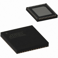
ATA5428-PLQW Atmel, ATA5428-PLQW Datasheet - Page 56

ATA5428-PLQW
Manufacturer Part Number
ATA5428-PLQW
Description
IC TXRX WIDEBND 433/868MHZ 48QFN
Manufacturer
Atmel
Specifications of ATA5428-PLQW
Frequency
433MHz, 868MHz
Data Rate - Maximum
20kbps
Modulation Or Protocol
ASK, FSK
Applications
Alarm and Security Systems, RKE
Power - Output
10dBm
Sensitivity
-112.5dBm
Voltage - Supply
2.4 V ~ 3.6 V or 4.4 V ~ 6.6 V
Current - Receiving
10.5mA
Current - Transmitting
10mA
Data Interface
PCB, Surface Mount
Antenna Connector
PCB, Surface Mount
Operating Temperature
-40°C ~ 85°C
Package / Case
48-VQFN Exposed Pad, 48-HVQFN, 48-SQFN, 48-DHVQFN
Operating Temperature (min)
-40C
Operating Temperature (max)
85C
Operating Temperature Classification
Industrial
Product Depth (mm)
7mm
Product Height (mm)
0.9mm
Product Length (mm)
7mm
Lead Free Status / RoHS Status
Lead free / RoHS Compliant
Memory Size
-
Lead Free Status / Rohs Status
Compliant
Other names
ATA5428-PLQHCT
ATA5428-PLQHCT
ATA5428-PLQWCT
ATA5428-PLQHCT
ATA5428-PLQWCT
Available stocks
Company
Part Number
Manufacturer
Quantity
Price
Company:
Part Number:
ATA5428-PLQW
Manufacturer:
LITELINK
Quantity:
106
Part Number:
ATA5428-PLQW
Manufacturer:
ATMEL/爱特梅尔
Quantity:
20 000
9.1.4
9.1.5
Figure 9-3.
56
ATA5423/ATA5425/ATA5428/ATA5429
RX_ACTIVE
Bit-check Mode
Configuration of the Bit Check
Demod_Out
Bit check
Timing Diagram for Complete Successful Bit Check (Number of Checked Bits: 3)
Start-up mode
T
Startup_Sig_Proc
In bit-check mode the incoming data stream is examined to distinguish between a valid signal
from a corresponding transmitter and signals due to noise. This is done by subsequent time
frame checks where the distance between 2 signal edges are continuously compared to a pro-
grammable time window. The maximum count of this edge-to-edge test before the transceiver
switches to receiving mode is also programmable.
Assuming a modulation scheme that contains 2 edges per bit, two time frame checks verify one
bit. This is valid for Manchester, Bi-phase and most other modulation schemes. The maximum
count of bits to be checked can be set to 0, 3, 6 or 9 bits via the variable N
register 5. This implies 0, 6, 12 and 18 edge-to-edge checks, respectively. If N
higher value, the transceiver is less likely to switch to receiving mode due to noise. In the pres-
ence of a valid transmitter signal, the bit check takes less time if N
In RX polling mode, the bit-check time is not dependent on N
Figure 9-3
As seen in
the edge-to-edge time t
limit T
the bit check will be terminated and the transceiver switches to sleep mode.
Figure 9-4.
Lim_max
shows an example where 3 bits are tested successfully.
Figure
, the check will be continued. If t
1/2 Bit
Valid Time Window for Bit Check
Demod_Out
9-4, the time window for the bit check is defined by two separate time limits. If
ee
1/2 Bit
is in between the lower bit-check limit T
Bit check mode
T
1/2 Bit
Bit-check
Bit check ok
T
T
Lim_max
1/2 Bit
Lim_min
t
ee
ee
is smaller than limit T
1/2 Bit
1/f
Sig
Bit-check
1/2 Bit
Lim_min
Bit-check
if no valid signal is present.
Lim_min
Receiving mode
and the upper bit-check
is set to a lower value.
or exceeds T
Bit-check
Bit-check
4841D–WIRE–10/07
is set to a
in control
Lim_max
,


