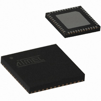
ATA5428-PLQW Atmel, ATA5428-PLQW Datasheet - Page 57

ATA5428-PLQW
Manufacturer Part Number
ATA5428-PLQW
Description
IC TXRX WIDEBND 433/868MHZ 48QFN
Manufacturer
Atmel
Specifications of ATA5428-PLQW
Frequency
433MHz, 868MHz
Data Rate - Maximum
20kbps
Modulation Or Protocol
ASK, FSK
Applications
Alarm and Security Systems, RKE
Power - Output
10dBm
Sensitivity
-112.5dBm
Voltage - Supply
2.4 V ~ 3.6 V or 4.4 V ~ 6.6 V
Current - Receiving
10.5mA
Current - Transmitting
10mA
Data Interface
PCB, Surface Mount
Antenna Connector
PCB, Surface Mount
Operating Temperature
-40°C ~ 85°C
Package / Case
48-VQFN Exposed Pad, 48-HVQFN, 48-SQFN, 48-DHVQFN
Operating Temperature (min)
-40C
Operating Temperature (max)
85C
Operating Temperature Classification
Industrial
Product Depth (mm)
7mm
Product Height (mm)
0.9mm
Product Length (mm)
7mm
Lead Free Status / RoHS Status
Lead free / RoHS Compliant
Memory Size
-
Lead Free Status / Rohs Status
Compliant
Other names
ATA5428-PLQHCT
ATA5428-PLQHCT
ATA5428-PLQWCT
ATA5428-PLQHCT
ATA5428-PLQWCT
Available stocks
Company
Part Number
Manufacturer
Quantity
Price
Company:
Part Number:
ATA5428-PLQW
Manufacturer:
LITELINK
Quantity:
106
Part Number:
ATA5428-PLQW
Manufacturer:
ATMEL/爱特梅尔
Quantity:
20 000
Figure 9-5.
4841D–WIRE–10/07
Bit-check counter
(Lim_min = 14, Lim_max = 24)
RX_ACTIVE
Demod_Out
Timing Diagram During Bit Check
Bit check
T
Start-up mode
Startup_Sig_Proc
For the best noise immunity, use of a low span between T
This is achieved using a fixed frequency at a 50% duty cycle for the transmitter preburst: a
“11111...” or a “10101...” sequence in Manchester or Bi-phase is a good choice. A good compro-
mise between sensitivity and susceptibility to noise regarding the expected edge-to-edge time,
t
and then N
the bit-check limits must be programmed according to the required span.
The bit-check limits are determined by means of the formula below:
Lim_min is defined by the bits Lim_min 0 to Lim_min 5 in control register 5.
Lim_max is defined by the bits Lim_max 0 to Lim_max 5 in control register 6.
Using the above formulas, Lim_min and Lim_max can be determined according to the required
T
minimum edge-to-edge time t
lower limit should be set to Lim_min
Lim_max = 63.
Figure
Lim_min = 14 and Lim_max = 24. The signal processing circuits are enabled during T
and T
that period. When the bit check becomes active, the bit-check counter is clocked with the cycle
T
Figure 9-5
limits defined by Lim_min and Lim_max at the occurrence of a signal edge. In
page 58
check also fails if CV_Lim reaches Lim_max. This is illustrated in
ee
XDCLK
Lim_min
, is a time window of ±38%; to get the maximum sensitivity the time window should be ±50%
0
Startup_Sig_Proc
.
, T
9-5,
1 2 3 4 5 6 7 8 1 2 3 4 5 6 7 8 9 101112131415161718 1 2 3 4 5 6 7 8 9 10 11
the bit check fails because the value CV_Lim is lower than the limit Lim_min. The bit
Lim_max
shows how the bit check proceeds if the bit-check counter value CV_Lim is within the
Bit-check
Figure
T
XDCLK
and T
. The output of the ASK/FSK demodulator (Demod_Out) is undefined during
6. Using preburst patterns that contain various edge-to-edge time periods,
9-6, and
T
T
ATA5423/ATA5425/ATA5428/ATA5429
XDCLK
Lim_min
Lim_max
. The time resolution defining T
= Lim_min
= (Lim_max -1)
ee
1/2 Bit
Figure 9-7
is defined in the section
Bit check mode
Bit check ok
T
illustrate the bit check for the bit-check limits
T
10. The maximum value of the upper limit is
Bit-check
XDCLK
T
XDCLK
1/2 Bit
Lim_min
“Receiving Mode” on page
Lim_min
and T
Figure 9-7 on page
12131415 1 2 3 4 5 6 7
and T
Bit check ok
Lim_max
Lim_max
1/2 Bit
is recommended.
is T
Figure 9-6 on
XDCLK
58.
Startup_PLL
59. The
. The
57


