FSBB15CH60C Fairchild Semiconductor, FSBB15CH60C Datasheet - Page 26
FSBB15CH60C
Manufacturer Part Number
FSBB15CH60C
Description
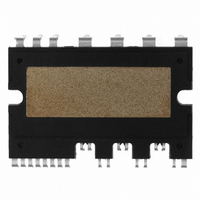
IC POWER MOD SPM 600V SPM27CC
Manufacturer
Fairchild Semiconductor
Series
SPM™r
Type
IGBTr
Specifications of FSBB15CH60C
Configuration
3 Phase
Current
15A
Voltage
600V
Voltage - Isolation
2500Vrms
Package / Case
SPM27CC
Transistor Polarity
N Channel
Dc Collector Current
15A
Collector Emitter Voltage Vces
2V
Power Dissipation Pd
55W
Collector Emitter Voltage V(br)ceo
600V
Operating Temperature Range
-40°C To
Operating Temperature (max)
150C
Operating Temperature (min)
-40C
Pin Count
27
Mounting
Through Hole
Case Length
44mm
Case Height
5.5mm
Screening Level
Automotive
Lead Free Status / RoHS Status
Lead free / RoHS Compliant
Available stocks
Company
Part Number
Manufacturer
Quantity
Price
Company:

Part Number:
FSBB15CH60C
Manufacturer:
CYPRESS
Quantity:
5 610
Part Number:
FSBB15CH60C
Manufacturer:
FSC/ONهڈ¯çœ‹è´§
Quantity:
20 000


6.2 General Interface Circuit Example
directly to a CPU.
Notes:
1. To avoid malfunction, the wiring of each input should be as short as possible. (less than 2-3cm)
2. By virtue of integrating an application specific type HVIC inside the Mini DIP SPM, direct coupling to
3. V
4. A C
5. The V
6. The input signals are Active-high configured. There is a internal 5kΩ pull-down resistor from each input
7. To prevent protection function errors, the R
8. The short-circuit protection time constant R
2008-03-03
CPU terminals without any opto-coupler or transformer isolation is possible.
logic power supply with approximately 4.7kΩ resistance. (reference Figure 6.1)
(pin7) and COM (pin2). (Example : if C
approximate equation of C
signal line to GND. When employing RC coupling circuits between the CPU and Mini DIP SPM select the
RC values such that the input signals will be compatible with the Mini DIP SPM turn-off/turn-on threshold
voltages.
FO
Figure 6.3 shows a typical application circuit of interface schematic with control signals connected
C
U
P
SP15
output is an open collector output. This signal line should be pulled up to the positive side of the 5V
FO
capacitance value approximately 7 times larger than bootstrap capacitor C
output pulse width is determined by the value of an external capacitor (C
FOD
pin in page 16 for calculation method.
Figure 6.3 Example of application circuit
(12) V
(19) V
(18) V
(17) IN
(20) V
(15) V
(14) V
(13) IN
(11) V
(10) V
(9) IN
(16) V
FOD
(7) C
(6) V
(5) IN
(4) IN
(3) IN
(2) COM
(1) V
(8) C
F
F
C
(UH)
and C
V4 Mini DIP SPM Application Note (2008-03-03)
B(W)
CC
S(W)
B(V)
CC
B(U)
CC
S(U)
FO
CC
S(V)
SC
FOD
(VH)
(WH)
(WL)
(VL)
(UL)
SC
= 33 nF, then t
should be set in the range of 1~2μsec.
26
SC
FAIRCHILD SEMICONDUCTOR - Smart Power Module
COM
IN
VB
VB
VCC
VB
VCC
COM
VCC
COM
IN
C(SC)
C(FOD)
VFO
IN(WL)
IN(VL)
IN(UL)
COM
VCC
IN
wiring should be as short as possible.
OUT(WL)
OUT(UL)
OUT(VL)
OUT
OUT
OUT
VS
V
VS
VS
SL
FO
= 1.8ms (typ.)). Please refer to the
N
N
W (26)
N
P (27)
V (25)
U (24)
W
V
U
(22)
(21)
(23)
BS
is recommended.
FOD
) between C
FOD
Related parts for FSBB15CH60C
Image
Part Number
Description
Manufacturer
Datasheet
Request
R

Part Number:
Description:
Fairchild Semiconductor [IGBT MODULE]
Manufacturer:
Fairchild Semiconductor
Datasheet:

Part Number:
Description:
Discrete Semiconductor Modules
Manufacturer:
Fairchild Semiconductor
Part Number:
Description:
Discrete Semiconductor Modules
Manufacturer:
Fairchild Semiconductor
Part Number:
Description:
This N-Channel MOSFET is produced using Fairchild Semiconductor’s advanced Power Trench® process
Manufacturer:
Fairchild Semiconductor
Datasheet:
Part Number:
Description:
This N-Channel MOSFET is produced using Fairchild Semiconductor’s advanced Power Trench® process
Manufacturer:
Fairchild Semiconductor
Datasheet:
Part Number:
Description:
This N-Channel MOSFET is produced using Fairchild Semiconductor’s advanced PowerTrench® process
Manufacturer:
Fairchild Semiconductor
Datasheet:
Part Number:
Description:
This N-Channel MOSFET is produced using Fairchild Semiconductor’s advanced PowerTrench® process
Manufacturer:
Fairchild Semiconductor
Datasheet:
Part Number:
Description:
This N-Channel MOSFET is produced using Fairchild Semiconductor’s advanced Power Trench® process
Manufacturer:
Fairchild Semiconductor
Datasheet:
Part Number:
Description:
This N-Channel logic Level MOSFETs are produced using Fairchild Semiconductor‘s advanced Power Trench® process that has been special tailored to minimize the on-state resistance and yet maintain superior switching performance
Manufacturer:
Fairchild Semiconductor
Datasheet:
Part Number:
Description:
This N-Channel MOSFET is produced using Fairchild Semiconductor’s advanced Power Trench® process
Manufacturer:
Fairchild Semiconductor
Datasheet:
Part Number:
Description:
This N-Channel SyncFET™ is produced using Fairchild Semiconductor’s advanced PowerTrench® process
Manufacturer:
Fairchild Semiconductor
Datasheet:
Part Number:
Description:
This N-Channel SyncFET™ is produced using Fairchild Semiconductor’s advanced PowerTrench® process
Manufacturer:
Fairchild Semiconductor
Datasheet:
Part Number:
Description:
This N-Channel SyncFET™ is produced using Fairchild Semiconductor’s advanced PowerTrench® process
Manufacturer:
Fairchild Semiconductor
Datasheet:
Part Number:
Description:
This N-Channel logic Level MOSFETs are produced using Fairchild Semiconductor‘s advanced Power Trench® process that has been special tailored to minimize the on-state resistance and yet maintain superior switching performance
Manufacturer:
Fairchild Semiconductor
Datasheet:
Part Number:
Description:
This N-Channel MOSFET is produced using Fairchild Semiconductor’s advanced Power Trench® process that has been especially tailored to minimize the on-state resistance and yet maintain superior switching performance
Manufacturer:
Fairchild Semiconductor
Datasheet: