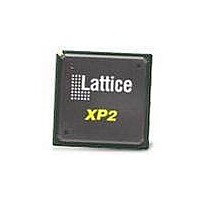
LFXP2-30E-5FN484C Lattice, LFXP2-30E-5FN484C Datasheet - Page 139

LFXP2-30E-5FN484C
Manufacturer Part Number
LFXP2-30E-5FN484C
Description
FPGA - Field Programmable Gate Array 30KLUTs 363 I/O Inst -on DSP 1.2V -5 Spd
Manufacturer
Lattice
Specifications of LFXP2-30E-5FN484C
Number Of Macrocells
29000
Number Of Programmable I/os
363
Data Ram Size
396288
Supply Voltage (max)
1.26 V
Maximum Operating Temperature
+ 85 C
Minimum Operating Temperature
0 C
Mounting Style
SMD/SMT
Supply Voltage (min)
1.14 V
Package / Case
FPBGA-484
Lead Free Status / RoHS Status
Lead free / RoHS Compliant
Available stocks
Company
Part Number
Manufacturer
Quantity
Price
Company:
Part Number:
LFXP2-30E-5FN484C
Manufacturer:
Lattice Semiconductor Corporation
Quantity:
10 000
- Current page: 139 of 341
- Download datasheet (10Mb)
LatticeXP2 sysCLOCK PLL
Lattice Semiconductor
Design and Usage Guide
CLKDIV Usage with Verilog - Example
module clkdiv_top(RST,CLKI,RELEASE,CDIV1,CDIV2,CDIV4,CDIV8);
input CLKI,RST,RELEASE;
output CDIV1,CDIV2,CDIV4,CDIV8;
CLKDIVB CLKDIBinst0 (.RST(RST),.CLKI(CLKI),.RELEASE(RELEASE),
.CDIV1(CDIV1),.CDIV2(CDIV2),.CDIV4(CDIV4),.CDIV8(CDIV8));
defparam CLKDIBint0.GXR = “DISABLED”;
endmodule
CLKDIV Example Circuits
The clock divider (CLKDIV) can divide a clock by 2 or 4 and drives a primary clock network. Clock dividers are use-
ful for providing the low speed FPGA clocks for I/O shift registers (x2, x4) and DDR (x2, x4) I/O logic interfaces.
Divide by 8 is provided for slow speed/low power operation.
To guarantee a synchronous transfer in the I/O logic the CLKDIV input clock must come from an edge clock and the
output drive from a primary clock. In this case, they are phase matched.
It is especially useful to synchronously reset the I/O logic when Mux/DeMux gearing is used in order to synchronize
the entire data bus as shown in Figure 9-14. Using the low skew characteristics of the edge clock routing a reset
can be provided to all bits of the data bus to synchronize the Mux/DeMux gearing.
The second circuit shows that a DLL can replace CLKDIV for x2 and x4 applications.
Figure 9-14. CLKDIV Application Example
Data
GEARING
D
Q
(2x)
8
16
Primary
ECLK
Clock
CLKDIV
RST
9-17
Related parts for LFXP2-30E-5FN484C
Image
Part Number
Description
Manufacturer
Datasheet
Request
R
Part Number:
Description:
FPGA LatticeXP2 Family 29000 Cells Flash Technology 1.2V 256-Pin FTBGA
Manufacturer:
LATTICE SEMICONDUCTOR
Datasheet:

Part Number:
Description:
IC DSP 30KLUTS 201I/O 256FTBGA
Manufacturer:
Lattice
Datasheet:

Part Number:
Description:
IC DSP 30KLUTS 201I/O 256FTBGA
Manufacturer:
Lattice
Datasheet:

Part Number:
Description:
IC DSP 30KLUTS 363I/O 484FPBGA
Manufacturer:
Lattice
Datasheet:

Part Number:
Description:
IC DSP 30KLUTS 363I/O 484FPBGA
Manufacturer:
Lattice
Datasheet:

Part Number:
Description:
IC DSP 30KLUTS 472I/O 672FPBGA
Manufacturer:
Lattice
Datasheet:

Part Number:
Description:
IC DSP 30KLUTS 472I/O 672FPBGA
Manufacturer:
Lattice
Datasheet:

Part Number:
Description:
IC FPGA 30KLUTS 201I/O 256-BGA
Manufacturer:
Lattice
Datasheet:

Part Number:
Description:
IC FPGA 30KLUTS 201I/O 256-BGA
Manufacturer:
Lattice
Datasheet:

Part Number:
Description:
IC FPGA 30KLUTS 472I/O 672-BGA
Manufacturer:
Lattice
Datasheet:

Part Number:
Description:
IC FPGA 30KLUTS 472I/O 672-BGA
Manufacturer:
Lattice
Datasheet:

Part Number:
Description:
IC FPGA 30KLUTS 201I/O 256-BGA
Manufacturer:
Lattice
Datasheet:

Part Number:
Description:
IC FPGA 30KLUTS 201I/O 256-BGA
Manufacturer:
Lattice
Datasheet:

Part Number:
Description:
IC FPGA 30KLUTS 201I/O 256-BGA
Manufacturer:
Lattice
Datasheet:

Part Number:
Description:
IC FPGA 30KLUTS 472I/O 672-BGA
Manufacturer:
Lattice
Datasheet:


