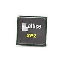
LFXP2-30E-5FN484C Lattice, LFXP2-30E-5FN484C Datasheet - Page 180

LFXP2-30E-5FN484C
Manufacturer Part Number
LFXP2-30E-5FN484C
Description
FPGA - Field Programmable Gate Array 30KLUTs 363 I/O Inst -on DSP 1.2V -5 Spd
Manufacturer
Lattice
Specifications of LFXP2-30E-5FN484C
Number Of Macrocells
29000
Number Of Programmable I/os
363
Data Ram Size
396288
Supply Voltage (max)
1.26 V
Maximum Operating Temperature
+ 85 C
Minimum Operating Temperature
0 C
Mounting Style
SMD/SMT
Supply Voltage (min)
1.14 V
Package / Case
FPBGA-484
Lead Free Status / RoHS Status
Lead free / RoHS Compliant
Available stocks
Company
Part Number
Manufacturer
Quantity
Price
Company:
Part Number:
LFXP2-30E-5FN484C
Manufacturer:
Lattice Semiconductor Corporation
Quantity:
10 000
- Current page: 180 of 341
- Download datasheet (10Mb)
Lattice Semiconductor
Figure 10-31. FIFO_DC without Output Registers, End of Data Write Cycle
In this case, the Almost Full flag is in the 2 location before the FIFO_DC is filled. The Almost Full flag is asserted
when the N-2 location is written, and the Full flag is asserted when the last word is written into the FIFO_DC.
Data_X data inputs do not get written as the FIFO_DC is full (the Full flag is high).
Note that the assertion of these flags is immediate and there is no latency when they go true.
Now let us look at the waveforms when the contents of the FIFO_DC are read out. Figure 10-32 shows the start of
the read cycle. RdEn goes high and the data read starts. The Full and Almost Full flags are de-asserted, as shown.
In this case, note that the de-assertion is delayed by two clock cycles.
RPReset
WrClock
RdClock
Almost
Almost
Empty
Empty
Reset
WrEn
RdEn
Data
Full
Full
Q
Data_N-2
Data_N-1
10-30
Invalid Q
Data_N
Data_X
LatticeXP2 Memory Usage Guide
Data_X
Related parts for LFXP2-30E-5FN484C
Image
Part Number
Description
Manufacturer
Datasheet
Request
R
Part Number:
Description:
FPGA LatticeXP2 Family 29000 Cells Flash Technology 1.2V 256-Pin FTBGA
Manufacturer:
LATTICE SEMICONDUCTOR
Datasheet:

Part Number:
Description:
IC DSP 30KLUTS 201I/O 256FTBGA
Manufacturer:
Lattice
Datasheet:

Part Number:
Description:
IC DSP 30KLUTS 201I/O 256FTBGA
Manufacturer:
Lattice
Datasheet:

Part Number:
Description:
IC DSP 30KLUTS 363I/O 484FPBGA
Manufacturer:
Lattice
Datasheet:

Part Number:
Description:
IC DSP 30KLUTS 363I/O 484FPBGA
Manufacturer:
Lattice
Datasheet:

Part Number:
Description:
IC DSP 30KLUTS 472I/O 672FPBGA
Manufacturer:
Lattice
Datasheet:

Part Number:
Description:
IC DSP 30KLUTS 472I/O 672FPBGA
Manufacturer:
Lattice
Datasheet:

Part Number:
Description:
IC FPGA 30KLUTS 201I/O 256-BGA
Manufacturer:
Lattice
Datasheet:

Part Number:
Description:
IC FPGA 30KLUTS 201I/O 256-BGA
Manufacturer:
Lattice
Datasheet:

Part Number:
Description:
IC FPGA 30KLUTS 472I/O 672-BGA
Manufacturer:
Lattice
Datasheet:

Part Number:
Description:
IC FPGA 30KLUTS 472I/O 672-BGA
Manufacturer:
Lattice
Datasheet:

Part Number:
Description:
IC FPGA 30KLUTS 201I/O 256-BGA
Manufacturer:
Lattice
Datasheet:

Part Number:
Description:
IC FPGA 30KLUTS 201I/O 256-BGA
Manufacturer:
Lattice
Datasheet:

Part Number:
Description:
IC FPGA 30KLUTS 201I/O 256-BGA
Manufacturer:
Lattice
Datasheet:

Part Number:
Description:
IC FPGA 30KLUTS 472I/O 672-BGA
Manufacturer:
Lattice
Datasheet:


