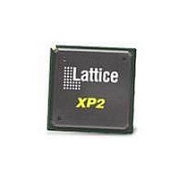
LFXP2-30E-5FN484C Lattice, LFXP2-30E-5FN484C Datasheet - Page 143

LFXP2-30E-5FN484C
Manufacturer Part Number
LFXP2-30E-5FN484C
Description
FPGA - Field Programmable Gate Array 30KLUTs 363 I/O Inst -on DSP 1.2V -5 Spd
Manufacturer
Lattice
Specifications of LFXP2-30E-5FN484C
Number Of Macrocells
29000
Number Of Programmable I/os
363
Data Ram Size
396288
Supply Voltage (max)
1.26 V
Maximum Operating Temperature
+ 85 C
Minimum Operating Temperature
0 C
Mounting Style
SMD/SMT
Supply Voltage (min)
1.14 V
Package / Case
FPBGA-484
Lead Free Status / RoHS Status
Lead free / RoHS Compliant
Available stocks
Company
Part Number
Manufacturer
Quantity
Price
Company:
Part Number:
LFXP2-30E-5FN484C
Manufacturer:
Lattice Semiconductor Corporation
Quantity:
10 000
- Current page: 143 of 341
- Download datasheet (10Mb)
Lattice Semiconductor
Figure 9-20. Timing Diagrams by DCS MODE (Cont.)
DCS Usage with VHDL - Example
COMPONENT DCS
-- synthesis translate_off
-- synthesis translate_on
END COMPONENT;
begin
DCSInst0: DCS
-- synthesis translate_off
attribute DCSMODE : string;
attribute DCSMODE of DCSinst0 : label is “POS”;
DCSOUT
DCSOUT
SEL
SEL
CLK1
CLK1
GENERIC
PORT
GENERIC MAP (
- Switch low @CLK1 falling edge.
- If SEL is low, output stays low at on
- Switch high @CLK1 rising edge.
- If SEL is low, output stays low high
CLK1 rising edge. SEL must not
change during setup prior to rising clock.
on CLK1 falling edge.
DCS MODE = HIGH_HIGH
DCS MODE = HIGH_LOW
(
DCSMODE : string :=
;
(
“POS”
9-21
DCSOUT
DCSOUT
SEL
SEL
CLK0
CLK0
- Switch low @CLK0 falling edge.
- If SEL is high, output stays low at
- Switch high @ CLK0 rising edge.
- If SEL is high, output stays high on
on CLK0 rising edge.
CLK0 falling edge.
DCS MODE = LOW_HIGH
DCS MODE = LOW_LOW
LatticeXP2 sysCLOCK PLL
Design and Usage Guide
Related parts for LFXP2-30E-5FN484C
Image
Part Number
Description
Manufacturer
Datasheet
Request
R
Part Number:
Description:
FPGA LatticeXP2 Family 29000 Cells Flash Technology 1.2V 256-Pin FTBGA
Manufacturer:
LATTICE SEMICONDUCTOR
Datasheet:

Part Number:
Description:
IC DSP 30KLUTS 201I/O 256FTBGA
Manufacturer:
Lattice
Datasheet:

Part Number:
Description:
IC DSP 30KLUTS 201I/O 256FTBGA
Manufacturer:
Lattice
Datasheet:

Part Number:
Description:
IC DSP 30KLUTS 363I/O 484FPBGA
Manufacturer:
Lattice
Datasheet:

Part Number:
Description:
IC DSP 30KLUTS 363I/O 484FPBGA
Manufacturer:
Lattice
Datasheet:

Part Number:
Description:
IC DSP 30KLUTS 472I/O 672FPBGA
Manufacturer:
Lattice
Datasheet:

Part Number:
Description:
IC DSP 30KLUTS 472I/O 672FPBGA
Manufacturer:
Lattice
Datasheet:

Part Number:
Description:
IC FPGA 30KLUTS 201I/O 256-BGA
Manufacturer:
Lattice
Datasheet:

Part Number:
Description:
IC FPGA 30KLUTS 201I/O 256-BGA
Manufacturer:
Lattice
Datasheet:

Part Number:
Description:
IC FPGA 30KLUTS 472I/O 672-BGA
Manufacturer:
Lattice
Datasheet:

Part Number:
Description:
IC FPGA 30KLUTS 472I/O 672-BGA
Manufacturer:
Lattice
Datasheet:

Part Number:
Description:
IC FPGA 30KLUTS 201I/O 256-BGA
Manufacturer:
Lattice
Datasheet:

Part Number:
Description:
IC FPGA 30KLUTS 201I/O 256-BGA
Manufacturer:
Lattice
Datasheet:

Part Number:
Description:
IC FPGA 30KLUTS 201I/O 256-BGA
Manufacturer:
Lattice
Datasheet:

Part Number:
Description:
IC FPGA 30KLUTS 472I/O 672-BGA
Manufacturer:
Lattice
Datasheet:


