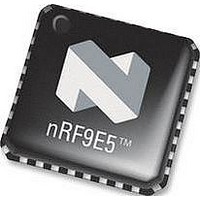
NRF9E5 NORDIC SEMICONDUCTOR, NRF9E5 Datasheet - Page 15

NRF9E5
Manufacturer Part Number
NRF9E5
Description
TRX, 430-928MHZ, MCU/ADC/PWM, SMD
Manufacturer
NORDIC SEMICONDUCTOR
Datasheet
1.NRF9E5.pdf
(108 pages)
Specifications of NRF9E5
Receiving Current
12.5mA
Transmitting Current
30mA
Data Rate
50Kbps
Frequency Range
430MHz To 928MHz
Modulation Type
GFSK
Rf Ic Case Style
QFN
No. Of Pins
32
Supply Voltage Range
1.9V To
Lead Free Status / RoHS Status
Lead free / RoHS Compliant
Available stocks
Company
Part Number
Manufacturer
Quantity
Price
Company:
Part Number:
NRF9E5C
Manufacturer:
NORDIC
Quantity:
5 000
Part Number:
NRF9E5C
Manufacturer:
NORDIC
Quantity:
20 000
PRODUCT SPECIFICATION
nRF9E5 Single Chip Transceiver with Embedded Microcontroller and ADC
6 DIGITAL I/O PORTS
The nRF9E5 has two I/O ports located at the default locations for P0 and P1 in standard
8051, but the ports are fully bi-directional CMOS and the direction of each pin is
controlled by a _DIR and an _ALT bit for each bit as shown in the table below.
6.1
During this period the internal reset is active (regardless of whether or not the clock is
running), all the port pins related to P0 are configured as inputs, whereas the inputs
related to P1 are configured as required for an SPI master. When program execution
starts, all ports are still configured as during reset, and the program will need to set the
_ALT and/or the _DIR register for the pins that need another direction.
6.2
P0_ALT and P0_DIR control the P0 port function in that order of priority. If the
alternate function for port P0.n is set (by P0_ALT.n = 1) the pin will be input or output
as required by the alternate function (UART, external interrupt, timer inputs or PWM
output), except that the UART RXD direction will still depend on P0_DIR.1.
To use INT0_N or INT1_N as interrupts, the corresponding alternate function must be
activated, P0_ALT.3 / P0_ALT.4. P0_ALT.5 / P0_ALT.6 can be set to use P0.5 / P0.6
as a timer 0 / 1 control. In that case the CPU samples these signal every 4 CPU clock
periods. When the P0_ALT.n is not set, bit ‘n’ of the port is a GPIO function with the
direction controlled by P0_DIR.n.
Main office: Nordic Semiconductor ASA - Vestre Rosten 81, N-7075 Tiller, Norway -Phone +4772898900 - Fax +4772898989
Revision: 1.3
I/O Port Behavior During RESET
Port 0 (P0)
EECSN
MISO
MOSI
SCK
P00
P01
P02
P03
P04
P05
P06
P07
Pin
Default function
SPI.dataout
SPI.datain
SPI.clock
P1.3
P0.0
P0.1
P0.2
P0.3
P0.4
P0.5
P0.6
P0.7
Table 8 Port functions.
Page 15 of 108
INT0_N (interrupt)
INT1_N (interrupt)
T2 (timer2 input)
T0 (timer0 input)
T1 (timer1 input)
RXD (UART)
TXD (UART)
Alternate=1
GTIMER
PWM
SPI_CTRL != 01
P1.2
P1.0
P1.1
P1.3
June 2006


