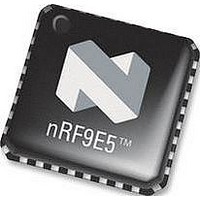
NRF9E5 NORDIC SEMICONDUCTOR, NRF9E5 Datasheet - Page 79

NRF9E5
Manufacturer Part Number
NRF9E5
Description
TRX, 430-928MHZ, MCU/ADC/PWM, SMD
Manufacturer
NORDIC SEMICONDUCTOR
Datasheet
1.NRF9E5.pdf
(108 pages)
Specifications of NRF9E5
Receiving Current
12.5mA
Transmitting Current
30mA
Data Rate
50Kbps
Frequency Range
430MHz To 928MHz
Modulation Type
GFSK
Rf Ic Case Style
QFN
No. Of Pins
32
Supply Voltage Range
1.9V To
Lead Free Status / RoHS Status
Lead free / RoHS Compliant
Available stocks
Company
Part Number
Manufacturer
Quantity
Price
Company:
Part Number:
NRF9E5C
Manufacturer:
NORDIC
Quantity:
5 000
Part Number:
NRF9E5C
Manufacturer:
NORDIC
Quantity:
20 000
PRODUCT SPECIFICATION
nRF9E5 Single Chip Transceiver with Embedded Microcontroller and ADC
18.8.1.4 Mode 3
In mode 3, Timer 0 operates as two 8-bit counters, and Timer 1 stops counting and holds
its value. As shown in Figure 20 Timer 0 – Mode 3, TL0 is configured as an 8-bit
counter controlled by the normal Timer 0 control bits. TL0 can count either CPU clock
cycles (divided by 4 or by 12) or high-to-low transitions on t0, as determined by the C/T
bit. The GATE function can be used to give counter enable control to the INT0_N
signal.
TH0 functions as an independent 8-bit counter. However, TH0 can count only CPU
clock cycles (divided by 4 or by 12). The Timer 1 control and flag bits (TR1 and TF1)
are used as the control and flag bits for TH0.
When Timer 0 is in mode 3, Timer 1 has limited usage because Timer 0 uses the Timer
1 control bit (TR1) and interrupt flag (TF1). Timer 1 can still be used for baud rate
generation and the Timer 1 count values are still available in the TL1 and TH1
registers.Control of Timer 1 when Timer 0 is in mode 3 is through the Timer 1 mode
bits. To turn Timer 1 on, set Timer 1 to mode 0, 1, or 2. To turn Timer 1 off, set it to
mode 3. The Timer 1 C/T bit and T1M bit are still available to Timer 1. Therefore,
Timer 1 can count CPU_clk/4, CPU_clk/12, or high-to-low transitions on the t1 pin. The
Timer 1 GATE function is also available when Timer 0 is in mode 3.
18.8.2 Timer Rate Control
The default timer clock scheme for the nRF9E5 timers is twelve CPU clock cycles per
increment, the same as in the standard 8051. However, in the nRF9E5, the instruction
cycle is four clock cycles.
Using the default rate (twelve clocks per timer increment) allows existing application
code with real-time dependencies, such as baud rate, to operate properly. However,
applications that require fast timing can set the timers to increment every four clock
cycles by setting bits in the Clock Control register (CKCON) at SFR location 0x8E,
described in Table 67 CKCON Register – SFR 0x.
The CKCON bits that control the timer clock rates are:
When a CKCON register bit is set to 1, the associated counter increments at four-clock
intervals. When a CKCON bit is cleared, the associated counter increments at twelve-
clock intervals. The timer controls are independent of each other. The default setting for
Main office: Nordic Semiconductor ASA - Vestre Rosten 81, N-7075 Tiller, Norway -Phone +4772898900 - Fax +4772898989
Revision: 1.3
CKCON bit Counter/Timer
P03/INT0_N
5
4
3
CPU_CLK
TR0
GATE
P0_ALT.3
TR1
P05/T0
Timer 2
Timer 1
Timer 0
Divide by 12
Divide by 4
Figure 20 Timer 0 – Mode 3.
0
1
T0M
Page 79 of 108
C/T
0
1
clk
clk
0
0
TL0
TH0
1
1
2
2
3
3
4
4
5
5
TF0
TF1
6
6
7
7
INT
INT
June 2006


