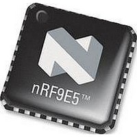
NRF9E5 NORDIC SEMICONDUCTOR, NRF9E5 Datasheet - Page 5

NRF9E5
Manufacturer Part Number
NRF9E5
Description
TRX, 430-928MHZ, MCU/ADC/PWM, SMD
Manufacturer
NORDIC SEMICONDUCTOR
Datasheet
1.NRF9E5.pdf
(108 pages)
Specifications of NRF9E5
Receiving Current
12.5mA
Transmitting Current
30mA
Data Rate
50Kbps
Frequency Range
430MHz To 928MHz
Modulation Type
GFSK
Rf Ic Case Style
QFN
No. Of Pins
32
Supply Voltage Range
1.9V To
Lead Free Status / RoHS Status
Lead free / RoHS Compliant
Available stocks
Company
Part Number
Manufacturer
Quantity
Price
Company:
Part Number:
NRF9E5C
Manufacturer:
NORDIC
Quantity:
5 000
Part Number:
NRF9E5C
Manufacturer:
NORDIC
Quantity:
20 000
PRODUCT SPECIFICATION
nRF9E5 Single Chip Transceiver with Embedded Microcontroller and ADC
1 ARCHITECTURAL OVERVIEW
This section will give a brief overview of each of the blocks in the block diagram in
Figure 1.
1.1
Microcontroller
The nRF9E5 microcontroller is instruction set compatible with the industry standard
8051. Instruction timing is slightly different from the industry standard, typically each
instruction will use from 4 to 20 clock cycles, compared with 12 to 48 for the
“standard”. The interrupt controller is extended to support 5 additional interrupt sources;
ADC, SPI, 2 for the radio and a wakeup function. There are also 3 timers that are 8052
compatible, plus some extensions, in the microcontroller core. An 8051 compatible
UART that can use timer1 or timer2 for baud rate generation in the traditional
asynchronous modes is included. The CPU is equipped with 2 data pointers to facilitate
easier moving of data in the XRAM area, which is a common 8051 extension. The
microcontroller clock is derived from the crystal oscillator.
1.1.1 Memory Configuration
The microcontroller has a 256-byte data ram (8052 compatible, with the upper half only
addressable by register indirect addressing). A small ROM of 512 bytes contains a
bootstrap loader that is executed automatically after power on reset or if initiated by
1
software later. The user program is normally loaded into a 4k byte RAM
from an
external serial EEPROM by the bootstrap loader. The 4k byte RAM may also (partially)
be used for data storage in some applications.
1.1.2 Boot EEPROM/FLASH
The program code for the device must be loaded from an external non-volatile memory.
The default boot loader expects this to be a “generic 25320” EEPROM with SPI
interface. These memories are available from several vendors with supply ranges down
to 1.8V. The SPI interface uses the pins MISO (from EEPROM SDO), SCK (to
EEPROM SCK), MOSI (to EEPROM SDI) and EECSN (to EEPROM CSN). When the
boot is completed, the MISO (P1.2), MOSI (P1.1) and SCK (P1.0) pins may be used for
other purposes such as other SPI devices or GPIO (General Purpose Input Output).
1.1.3 Register Map
The SFRs (Special Function Registers) control several of the features of the nRF9E5.
Most of the nRF9E5 SFRs are identical to the standard 8051 SFRs. However, there are
additional SFRs that control features that are not available in the standard 8051.
The SFR map is shown in Table 3. The registers with grey background are registers with
industry standard 8051 behavior. Note that the function of P0, P1 and P2 are somewhat
different from the “standard” even if the conventional addresses (0x80, 0x90 and 0xA0)
are used.
1
Optionally this 4k block of memory can be configured as 2k mask ROM and 2k RAM or 4k mask ROM
Main office: Nordic Semiconductor ASA - Vestre Rosten 81, N-7075 Tiller, Norway -Phone +4772898900 - Fax +4772898989
Revision: 1.3
Page 5 of 108
June 2006


