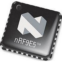
NRF9E5 NORDIC SEMICONDUCTOR, NRF9E5 Datasheet - Page 74

NRF9E5
Manufacturer Part Number
NRF9E5
Description
TRX, 430-928MHZ, MCU/ADC/PWM, SMD
Manufacturer
NORDIC SEMICONDUCTOR
Datasheet
1.NRF9E5.pdf
(108 pages)
Specifications of NRF9E5
Receiving Current
12.5mA
Transmitting Current
30mA
Data Rate
50Kbps
Frequency Range
430MHz To 928MHz
Modulation Type
GFSK
Rf Ic Case Style
QFN
No. Of Pins
32
Supply Voltage Range
1.9V To
Lead Free Status / RoHS Status
Lead free / RoHS Compliant
Available stocks
Company
Part Number
Manufacturer
Quantity
Price
Company:
Part Number:
NRF9E5C
Manufacturer:
NORDIC
Quantity:
5 000
Part Number:
NRF9E5C
Manufacturer:
NORDIC
Quantity:
20 000
PRODUCT SPECIFICATION
nRF9E5 Single Chip Transceiver with Embedded Microcontroller and ADC
Table 63 lists the functions of the bits in the PSW register.
Bit
PSW.7
PSW.6
PSW.5
PSW.4
PSW.3
PSW.2
PSW.1
PSW.0
Main office: Nordic Semiconductor ASA - Vestre Rosten 81, N-7075 Tiller, Norway -Phone +4772898900 - Fax +4772898989
Revision: 1.3
Function
CY - Carry flag. Set to 1 when last arithmetic operation resulted in a carry (during
addition) or borrow (during subtraction); otherwise cleared to 0 by all arithmetic
operations.
AC - Auxiliary carry flag. Set to 1 when last arithmetic operation resulted in a carry into
(during addition) or borrow from (during subtraction) the high-order nibble; otherwise
cleared to 0 by all arithmetic operations.
F0 - User flag 0. Bit-addressable, general purpose flag for software control.
RS1 - Register bank select bit 1. Used with RS0 to select a register blank in internal
RAM.
RS0 - Register bank select bit 0, decoded as:
OV - Overflow flag. Set to 1 when last arithmetic operation resulted in a carry (addition),
borrow (subtraction), or overflow (multiply or divide); otherwise cleared to 0 by all
arithmetic operations.
F1 - User flag 1. Bit-addressable, general purpose flag for software control.
P - Parity flag. Set to 1 when modulo-2 sum of 8 bits in accumulator is 1 (odd parity);
cleared to 0 on even parity.
RS1 RS0 Bank selected
0
0
1
1
0
1
0
1
Table 63 PSW Register – SFR 0xD0.
Register bank 0, addresses 0x00-0x07
Register bank 1, addresses 0x08-0x0F
Register bank 2, addresses 0x10-0x17
Register bank 3, addresses 0x18-0x1F
Page 74 of 108
June 2006


