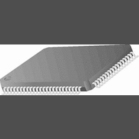
CR16MCS9VJE8 National Semiconductor, CR16MCS9VJE8 Datasheet - Page 123

CR16MCS9VJE8
Manufacturer Part Number
CR16MCS9VJE8
Description
16-Bit Microcontroller IC
Manufacturer
National Semiconductor
Datasheet
1.CR16MCS9VJE8.pdf
(156 pages)
Specifications of CR16MCS9VJE8
Controller Family/series
CR16X
Core Size
16 Bit
Program Memory Size
64K X 8 Flash
Digital Ic Case Style
PQFP
No. Of Pins
80
Mounting Type
Surface Mount
Clock Frequency
25MHz
Lead Free Status / RoHS Status
Contains lead / RoHS non-compliant
Available stocks
Company
Part Number
Manufacturer
Quantity
Price
Company:
Part Number:
CR16MCS9VJE8
Manufacturer:
ON
Quantity:
8 917
Company:
Part Number:
CR16MCS9VJE8-CBB
Manufacturer:
ON
Quantity:
846
Company:
Part Number:
CR16MCS9VJE8-CBC
Manufacturer:
ON
Quantity:
109
Company:
Part Number:
CR16MCS9VJE8-CBD
Manufacturer:
ON
Quantity:
17
Company:
Part Number:
CR16MCS9VJE8-CBE
Manufacturer:
ON
Quantity:
1 950
23.0 Memory Map
The CompactRISC architecture supports a uniform linear ad-
dress space of 2 megabytes. The device implementation of
this architecture uses only the lowest 128K bytes of address
space, ranging from 0000 to 1FFFF hex. Table42 is a mem-
ory map showing the types of memory and peripherals that
occupy this memory space. Address ranges not listed in the
table are reserved and should not be read or written.
0000-7FFF
8000-BFFF
C000-CBFF
E000-E5FF
E800-EFFF
F000-F07F
F400-F7FF
F800-FAFF
FB00-FB06
FB00-FBFF
FB10-FB16
FC00-FFFF
FC40-FC8A
FCA0-FCA8
FCC0-FCC8
FF00-FF08
FD20-FD28
FE00-FE1E
FE40-FE4E
FE60-FE66
FE80-FE8E
FEC0-FECA
FEE0-FEE8
FF20-FF2A
FF40-FF50
FF60-FF70
FF80-FFA4
FFC0-FFD0
FFE0-FFE0
1C000-1FFFF
a
. 32K ROM or Flash, size depends on device specifications.
Range (hex)
Address
Table 42 Device Memory Map
Flash Program Memory
Flash Program Memory (48K bytes)
Static RAM (3K bytes)
ISP Memory(1.5K bytes)
Lower Endurance Flash EEPROM Data
Memory (2K bytes)
High Endurance Flash EEPROM Data
Memory (128 bytes)
CAN buffers and registers (1K bytes)
BIU Peripherals (768 bytes)
Port B registers
I/O Expansion + Ports PB & PC (256bytes)
Port C registers
Peripherals and other I/O Ports (1K bytes)
Clock, Power Management, and Wake-Up
registers
Port G registers
Port H registers
Port L registers
Port F registers
Interrupt Control Unit registers
USART 1 registers
MICROWIRE registers
USART 2 registers
ACCESS.bus registers
Port I registers
Timer and WATCHDOG registers
Multi-function Timer1 registers
Multi-function Timer2 registers
Versatile Timer Unit registers
A/D Converter registers
Analog Comparator register
Flash Program Memory (16K bytes)
Description
a
b
123
Table43 is a detailed memory map showing the specific
memory address of the memory, I/O ports, and registers. The
table shows the starting address, the size, and a brief de-
scription of each memory block and register. For detailed in-
formation on using these memory locations, see the
applicable sections in the data sheet.
All addresses not listed in the table are reserved and should
not be read or written. An attempt to access an unlisted ad-
dress will have unpredictable results.
Each byte-wide register occupies a single address and can
be accessed only in a byte-wide transaction. Each word-wide
register occupies two consecutive memory addresses and
can be accessed only in a word-wide transaction. Both the
byte-wide and word-wide registers reside at word boundaries
(even addresses). Thus, each byte-wide register uses only
the lowest eight bits of the internal data bus.
Most device registers are read/write registers. However,
some registers are read-only or write-only, as indicated in the
table. An attempt to read a write-only register or to write a
read-only register will have unpredictable results.
When the software writes to a register in which one or more
bits are reserved, it must write a zero to each reserved bit un-
less indicated otherwise in the description of the register.
Reading a reserved bit returns an undefined value.
www.national.com


