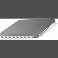
CR16MCS9VJE8 National Semiconductor, CR16MCS9VJE8 Datasheet - Page 66

CR16MCS9VJE8
Manufacturer Part Number
CR16MCS9VJE8
Description
16-Bit Microcontroller IC
Manufacturer
National Semiconductor
Datasheet
1.CR16MCS9VJE8.pdf
(156 pages)
Specifications of CR16MCS9VJE8
Controller Family/series
CR16X
Core Size
16 Bit
Program Memory Size
64K X 8 Flash
Digital Ic Case Style
PQFP
No. Of Pins
80
Mounting Type
Surface Mount
Clock Frequency
25MHz
Lead Free Status / RoHS Status
Contains lead / RoHS non-compliant
Available stocks
Company
Part Number
Manufacturer
Quantity
Price
Company:
Part Number:
CR16MCS9VJE8
Manufacturer:
ON
Quantity:
8 917
Company:
Part Number:
CR16MCS9VJE8-CBB
Manufacturer:
ON
Quantity:
846
Company:
Part Number:
CR16MCS9VJE8-CBC
Manufacturer:
ON
Quantity:
109
Company:
Part Number:
CR16MCS9VJE8-CBD
Manufacturer:
ON
Quantity:
17
Company:
Part Number:
CR16MCS9VJE8-CBE
Manufacturer:
ON
Quantity:
1 950
www.national.com
buffer consists of the 16-bit shifter and a buffer, called the
read buffer.
The 16-bit shifter loads the read buffer with new data when
the data transfer sequence is completed and previous data in
the read buffer has been read. In master mode, an Overrun
error occurs when the read buffer is full, the 16-bit shifter is
full and a new data transfer sequence starts.
When 8-bit mode is selected, the lower byte of the shift reg-
ister is loaded into the lower byte of the read buffer and the
read buffer’s higher byte remains unchanged.
The “Receive Buffer Full” (MRBF) bit indicates if the MWDAT
register holds valid data. The MOVR bit indicates that an
overrun condition has occurred.
17.1.3
The “MICROWIRE Busy” (MBSY) bit indicates whether the
MWDAT register can be written. All write operations to the
MWDAT register update the shifter while the data contained in
the read buffer is not affected. Undefined results will occur if
the MWDAT register is written to while the MBSY bit is set to 1.
17.1.4
Two clocking modes are supported: the normal mode and the
alternate mode.
In the normal mode, the output data, which is transmitted on
the MDODI pin (master mode) or the MDIDO pin (slave
mode), is clocked out on the falling edge of the shift clock
MSK. The input data, which is received via the MDIDO pin
System Clock
Interrupt Request
Writing
Clocking Modes
Read Data
Write Data
Clock Prescaler + Select
Data In
MSK
16-bit Shift Register
16-bit Read Buffer
8
Figure 25. MICROWIRE Block Diagram
Control + Status
8
MWDAT
66
Data Out
(master mode) or the MDODI pin (slave mode), is sampled
on the rising edge of MSK.
In the alternate mode, the output data is shifted out on the ris-
ing edge of MSK on the MDODI pin (master mode) or MDIDO
pin (slave mode). The input data, which is received via MDI-
DO pin (master mode) or MDODI pin (slave mode), is sam-
pled on the falling edge of MSK.
The clocking modes are selected with the MSKM bit. The
MIDL bit allows selection of the value of MSK when it is idle
(when there is no data being transferred). Various MSK clock
frequencies can be programmed via the MCDV bits. Figures
27, 28, 29, and 30 show the data transfer timing for the nor-
mal and the alternate modes with the MIDL bit equal to 0 and
equal to 1.
Note that when data is shifted out on MDODI (master mode)
or MDIDO (slave mode) on the leading edge of the MSK
clock, bit 14 (16-bit mode) is shifted out on the second lead-
ing edge of the MSK clock. When data are shifted out on
MDODI (master mode) or MDIDO (slave mode) on the trail-
ing edge of MSK, bit 14 (16-bit mode) is shifted out on the first
trailing edge of MSK.
17.2
In Master mode, the MSK pin is an output for the shift clock,
MSK. When data is written to the (MWnDAT register), eight
or sixteen MSK clocks, depending on the mode selected, are
generated to shift the eight or sixteen bits of data and then
MASTER MODE
Master
Master
Slave
Master
Slave
MCS
MDODI
MDIDO
MSK


