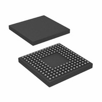
ADSP-BF531SBBC400 Analog Devices Inc, ADSP-BF531SBBC400 Datasheet - Page 31

ADSP-BF531SBBC400
Manufacturer Part Number
ADSP-BF531SBBC400
Description
IC,MICROPROCESSOR,32-BIT,CMOS,BGA,160PIN,PLASTIC
Manufacturer
Analog Devices Inc
Series
Blackfin®r
Type
Fixed Pointr
Datasheet
1.ADSP-BF531SBSTZ400.pdf
(12 pages)
Specifications of ADSP-BF531SBBC400
Rohs Status
RoHS non-compliant
Interface
SPI, SSP, UART
Clock Rate
400MHz
Non-volatile Memory
ROM (1 kB)
On-chip Ram
52kB
Voltage - I/o
1.8V, 2.5V, 3.3V
Voltage - Core
1.20V
Operating Temperature
-40°C ~ 85°C
Mounting Type
Surface Mount
Package / Case
160-CSPBGA
Device Core Size
16b
Architecture
Modified Harvard
Format
Fixed Point
Clock Freq (max)
400MHz
Mips
400
Device Input Clock Speed
400MHz
Operating Supply Voltage (typ)
1.2/1.8/2.5/3.3V
Operating Supply Voltage (min)
0.8/1.75V
Operating Supply Voltage (max)
1.32/3.6V
Operating Temp Range
-40C to 85C
Operating Temperature Classification
Industrial
Mounting
Surface Mount
Pin Count
160
Package Type
CSPBGA
Package
160CSP-BGA
Numeric And Arithmetic Format
Fixed-Point
Maximum Speed
400 MHz
Device Million Instructions Per Second
400 MIPS
For Use With
ADZS-BF533-EZLITE - KIT W/BOARD EVAL FOR ADSP-BF533
Lead Free Status / Rohs Status
Not Compliant
Available stocks
Company
Part Number
Manufacturer
Quantity
Price
Company:
Part Number:
ADSP-BF531SBBC400
Manufacturer:
ADI
Quantity:
329
Company:
Part Number:
ADSP-BF531SBBC400
Manufacturer:
Analog Devices Inc
Quantity:
10 000
Part Number:
ADSP-BF531SBBC400
Manufacturer:
ADI/亚德诺
Quantity:
20 000
Silicon Anomaly List
54.
55.
DESCRIPTION:
When the Core Clock is not at least twice as fast as the the System Clock, 32-bit or wider writes to SDRAM memory may be lost. Note that
since cache victims are effectively 256 bit wide writes, cache victimization will also trigger this anomaly.
WORKAROUND:
Either:
1) Make sure that the Core Clock (CCLK) is at least twice as fast as the System Clock (SCLK)
or
2) Make sure all external memory writes are 16 bits wide or less:
If using data cache, the Write Through policy should be used since there is no cache victimization in this mode.
APPLIES TO REVISION(S):
0.3, 0.4, 0.5
DESCRIPTION:
The PPI timing diagrams in the processor data sheet only apply to PPI modes where the PPI_DELAY register is set to zero.
WORKAROUND:
For non-zero values of the PPI_DELAY register, the following information applies:
In the data sheet, when POLC = 0, the frame sync is sampled on the falling edge of the PPI clock and the corresponding setup time is
shown relative to this edge. When the PPI_DELAY register is a non-zero value, the frame sync setup time increases by one half the period
of the PPI clock. The delay starts counting at the point on the existing diagrams where data is shown to be sampled.
In the data sheet, when POLC = 1, the frame sync is sampled on the rising edge of the PPI clock and the corresponding setup time is
shown relative to this edge. When the PPI_DELAY register is a non-zero value, the frame sync setup time increases by one half the period
of the PPI clock. The delay starts counting at the point on the existing diagrams where data is shown to be sampled.
APPLIES TO REVISION(S):
0.3, 0.4, 0.5, 0.6
05000273 - Writes to Synchronous SDRAM Memory May Be Lost:
05000276 - Timing Requirements Change for External Frame Sync PPI Modes with Non-Zero PPI_DELAY:
W[P2] = R0;
B[P2] = R0;
// 16-bit write
//
8-bit write
NR003532D | Page 31 of 45 | July 2008
ADSP-BF531/BF532/BF533


